Formation method of transistors

A transistor and semiconductor technology, which is applied in the fields of semiconductor devices, semiconductor/solid-state device manufacturing, electrical components, etc., can solve the problems of complex formation process and unstable transistor performance, and achieve the effect of simplifying process steps.

Active Publication Date: 2014-12-17
SEMICON MFG INT (SHANGHAI) CORP
View PDF6 Cites 4 Cited by
  • Summary
  • Abstract
  • Description
  • Claims
  • Application Information

AI Technical Summary

Problems solved by technology

[0005] In the prior art, the "gate-last" process is usually used to form high-K metal gate transistors with thinner gate dielectric layers, and the "gate-front" process is used to form polysilicon gate transistors with thicker gate dielectric layers. The formation process is relatively complicated, and The performance of transistors formed by the "gate-last" process is not stable enough

Method used


Image

  • Formation method of transistors
  • Formation method of transistors
  • Formation method of transistors

Examples


Embodiment Construction

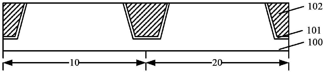
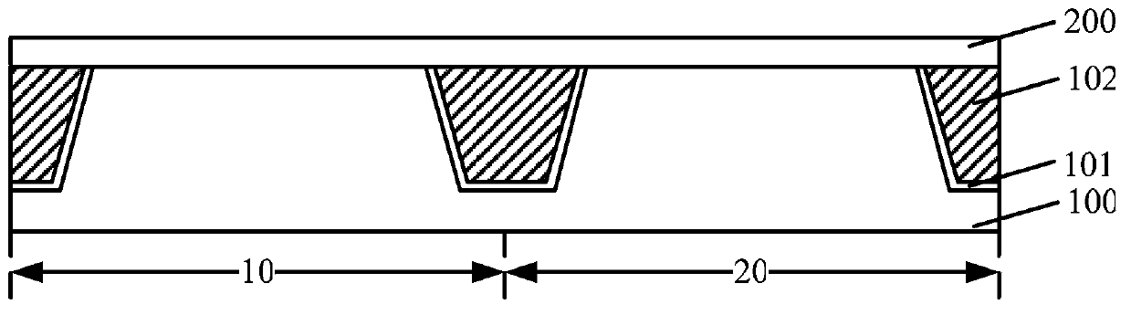
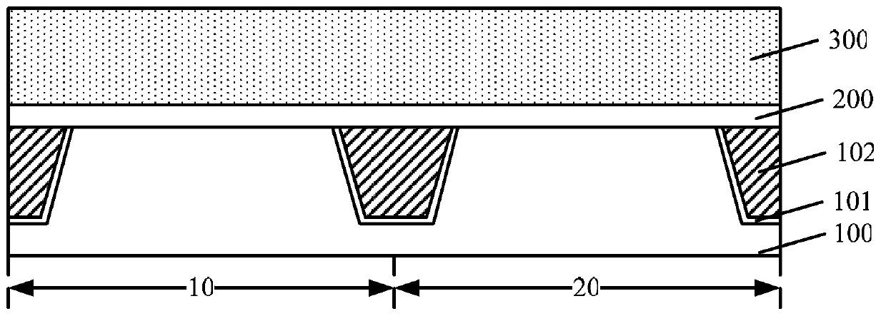
[0031] As mentioned in the background art, the process steps of forming transistors with gate dielectric layers of different thicknesses in the prior art are relatively complicated, and the performance of the formed transistors is not stable enough.

[0032] The inventors found that in the current process of forming a high-K metal gate transistor with a thinner gate dielectric layer by using the gate-last process, the process of removing the dummy gate dielectric layer generally adopts a wet etching process, because the dummy gate The materials of the dielectric layer and the interlayer dielectric layer are relatively close, and the material density of the dummy gate dielectric layer is generally greater than that of the interlayer dielectric layer, so in the wet etching process, the etching rate of the interlayer dielectric layer will be greater than that of the dummy gate dielectric layer. The etch rate of the gate dielectric layer will cause a large loss to the interlayer di...


PUM

PropertyMeasurementUnit
Thicknessaaaaaaaaaa

Abstract

Disclosed is a formation method of transistors. The formation method includes: providing a semiconductor substrate which comprises a first area and a second area; forming a pseudo gate dielectric material layer on the surface of the semiconductor substrate; forming a pseudo gate on the surface of the pseudo gate dielectric material layer of the first area, and forming a second gate on the surface of the pseudo gate dielectric material layer of the second area; etching the pseudo gate dielectric material layer and forming pseudo gate dielectric layers located under the pseudo gate and a second gate dielectric layer under the second gate; forming a first source / drain region in the first area, and forming a second source / drain region in the second area; forming an interlayer dielectric layer on the surface of the semiconductor substrate; removing the pseudo gate and the pseudo gate dielectric layers to form a groove. The method for removing the pseudo gate dielectric layer includes: adopting dry etching to remove part of the pseudo gate dielectric layers in the thickness direction, and adopting wet etching to remove the rest pseudo gate dielectric layers; forming a first gate structure in the groove. By the formation method, steps can be simplified, and performance of the transistors can be improved.

Description

technical field [0001] The invention relates to the technical field of semiconductors, in particular to a method for forming a transistor. Background technique [0002] With the continuous improvement of the integration level of semiconductor devices and the reduction of technology nodes, the traditional gate dielectric layer continues to become thinner, and the leakage of transistors increases accordingly, causing problems such as waste of power consumption of semiconductor devices. In order to solve the above problems, the prior art provides a solution of replacing the polysilicon gate with a metal gate. Among them, the "gate last" process is a main process for forming high-K metal gate transistors. [0003] The existing method for forming a high-K metal gate transistor using a gate-last process includes: providing a semiconductor substrate on which a dummy gate structure is formed and located on the semiconductor substrate and covering the dummy gate structure The inter...

Claims


Application Information

Patent Timeline
IPC IPC(8): H01L21/28H01L21/336H01L21/8234
CPCH01L21/31111H01L21/823462H01L29/4236H01L29/42364
Inventor 谢欣云
Owner SEMICON MFG INT (SHANGHAI) CORP
Why Eureka
Try Eureka