
Method for manufacturing panels of color touch screens

A touch screen and panel technology, applied in the input/output process of data processing, instruments, electrical digital data processing, etc., can solve the problems of product scrapping, large environmental pollution of hydrofluoride, high scrap rate, etc., and achieve suitable mass production, The manufacturing process is easier to control and the effect of improving the yield rate

Inactive Publication Date: 2014-12-03
凯盛科技股份有限公司
View PDF2 Cites 3 Cited by
  • Summary
  • Abstract
  • Description
  • Claims
  • Application Information

AI Technical Summary

Problems solved by technology

Although this preparation method can obtain the color touch screen panel with the above structure, it still has the following problems: due to the need to use hydrofluoride in the preparation process, and the warming potential of hydrofluoride is 23000 times that of carbon dioxide, its impact on climate change It has a very large impact, so hydrofluoride is very polluting to the environment and must be strictly controlled, and hydrofluoride can corrode the glass substrate, once the glass substrate is damaged, the product will be scrapped, so the scrap rate of this preparation method relatively high

Method used


Image

  • Method for manufacturing panels of color touch screens
  • Method for manufacturing panels of color touch screens
  • Method for manufacturing panels of color touch screens

Examples


Embodiment Construction

[0017] The present invention will be further described below in conjunction with accompanying drawing:

[0018] This section generally describes the materials and test methods used in the experiments of the present invention. While many of the materials and manipulations which are employed for the purposes of the invention are well known in the art, the invention has been described here in as much detail as possible. It will be clear to those skilled in the art that in the following, unless otherwise specified, the materials, equipment and operation methods used in the present invention are well known in the art.

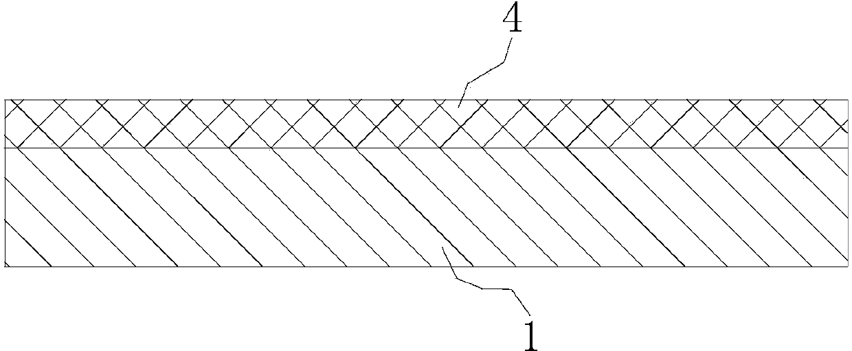
[0019] see figure 1 , the color touch screen panel prepared by the existing preparation method and the preparation method of the color touch screen panel of the present invention includes a substrate 1 , an optical film layer 2 covering the substrate 1 and an opaque insulating layer 3 covering the optical film layer 2 .

[0020] see Figure 2 to Figure 7 , the pr...


PUM


Abstract

The invention discloses a method for manufacturing panels of color touch screens. The method includes steps of providing substrates; coating positive photoresist layers on the substrates; exposing, developing and solidifying the positive photoresist layers, removing exposed portions of the positive photoresist layers by means of developing and reserving unexposed portions of the positive photoresist layers; forming optical film layers on the reserved portions of the positive photoresist layers and certain regions on the substrates; removing films on the reserved portions of the positive photoresist layers so as to remove first certain portions of the optical film layers, and reserving second certain portions of the optical film layers; forming nontransparent insulating layers on the reserved portions of the optical film layers. The certain regions on the substrates correspond to the portions, which are removed by means of developing, of the positive photoresist layers. The first certain portions of the optical film layers cover the reserved portions of the positive photoresist layers. The second certain portions of the optical film layers cover the regions, which correspond to the certain portions of the positive photoresist layers, of the substrates, and the certain portions of the positive photoresist layers are removed by means of developing. The method has the advantages that problems of environmental pollution and corrosion on substrates made of glass materials due to hydrofluoride can be solved, accordingly, the yield can be increased, manufacturing procedures are easy to control, and the method is suitable for large-scale production.

Description

technical field [0001] The invention relates to the technical field of touch screens, in particular to a method for preparing a color touch screen panel. Background technique [0002] The touch screen manufacturing technology is becoming more and more mature. The OGS (one glass solution) method of making the touch unit on the touch screen cover is the mainstream way to realize the ultra-thin touch screen. With the development of touch screen technology, the appearance is colorful and personalized. into a development trend. [0003] An existing color touch screen panel includes a substrate, an optical film layer covering the substrate, and an opaque insulating layer covering the optical film layer. The patterns of the optical film layer and the opaque insulating layer are the same and corresponding. When light passes through the When the substrate irradiates the optical film, a part of the light will be reflected by the contact interface between the optical film and the subs...

Claims


Application Information

Patent Timeline
Patent Type & Authority Applications(China)
IPC IPC(8): G06F3/041
Inventor 茆令文樊黎虎曹绪文张少波乔辉
Owner 凯盛科技股份有限公司
Learn More