Card and card production method
一种制造方法、基板的技术,应用在机器使用的记录载体、支撑结构上的电路布置、其他印刷电路零部件等方向,能够解决加热、加压不充分、生产效率降低、长时间挤压等问题,达到提高外观品质的效果
- Summary
- Abstract
- Description
- Claims
- Application Information
AI Technical Summary
Problems solved by technology
Method used
Image

Examples
no. 1 Embodiment approach
[0044] Hereinafter, a first embodiment of the present invention will be described with reference to the drawings and the like.
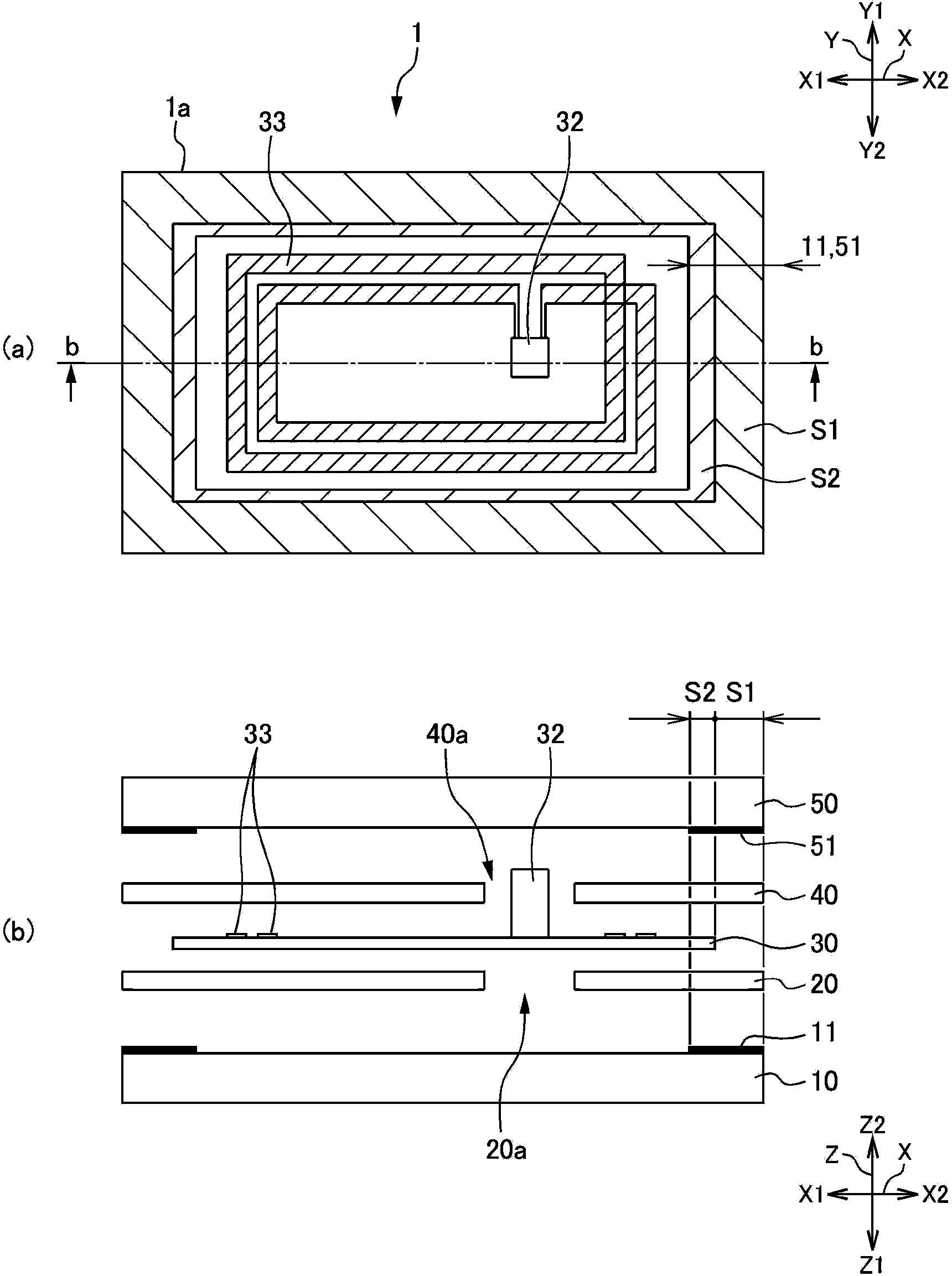
[0045] figure 1 It is a plan view and a cross-sectional view of the card 1 of the first embodiment.
[0046] figure 1 (a) is a plan view of the card 1 .
[0047] figure 1 (b) is a cross-sectional view illustrating the layer structure of the card 1 ( figure 1 (a) b-b sectional view) shows the state before joining each layer.
[0048] In the embodiments and drawings, a drawing in which the card surface and the like are viewed with the normal direction of the card surface as the vertical direction Z is referred to as a plan view. In addition, the long side direction of the card 1 in plan view is defined as the left-right direction X, and the short side direction is defined as the vertical direction Y. The shape in the top view is called the proper top view shape.
[0049] In addition, in each drawing, in order to clearly show the structure etc. of ...
no. 2 Embodiment approach
[0154] Next, a second embodiment of the present invention will be described.
[0155] In the description of the following embodiment and the drawings, the same reference numerals are attached to the parts that realize the same functions as those of the above-mentioned first embodiment, or the same reference numerals are assigned at the end, and repeated descriptions are appropriately omitted.
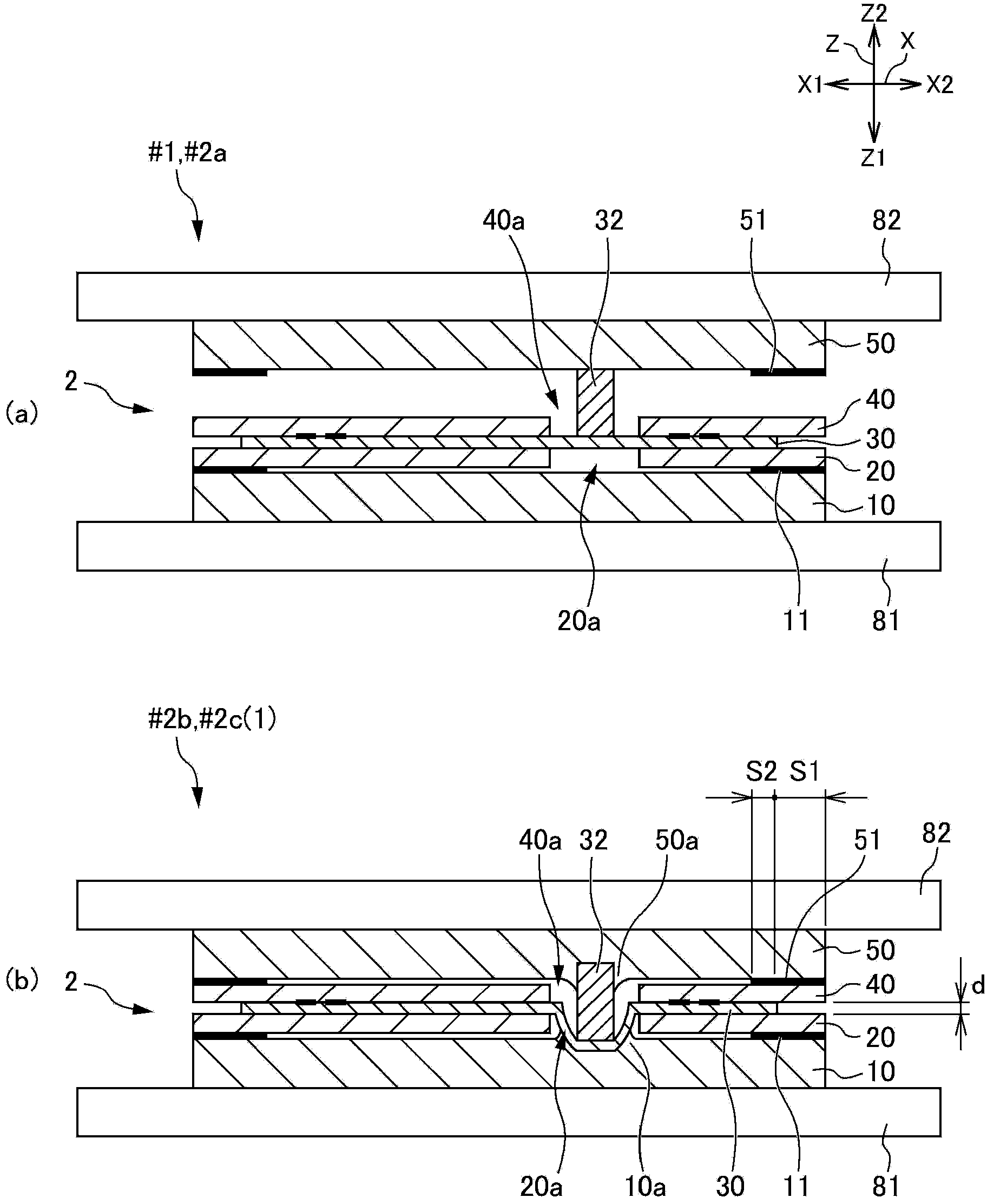
[0156] Figure 8 It is explanatory drawing of the layer structure of the card 201 of 2nd Embodiment.
[0157] Figure 9 It is explanatory drawing of the manufacturing process of the card 201 of 2nd Embodiment.
[0158] Figure 9 (a) is with Figure 4 (c) Corresponding figure.
[0159] Figure 9 (b) is with Figure 4 (d) Corresponding figure.
[0160] Figure 9 (c) is with Figure 5 (f) Corresponding figure.
[0161] Such as Figure 8 As shown, since the thickness of the IC chip 232 is thinner than that of the first embodiment, the card 201 does not include the upper spacer.
...
no. 3 Embodiment approach
[0167] Next, a third embodiment of the present invention will be described.
[0168] Figure 10 It is explanatory drawing of the layer structure and manufacturing process of the card 301 of 3rd Embodiment.
[0169] Such as Figure 10 As shown in (a), the module substrate 330 is only mounted with wiring patterns 333 and thin electronic components (not shown), and is not mounted with thick electronic components such as IC chips. Therefore, the upper spacer and the lower spacer are not required for the card 301 , and the lower layer 310 and the upper layer 350 are directly stacked on the module substrate 330 .
[0170] Even in this case, the thickness adjustment layers 311 and 351 of the card 301 can increase the surface pressure between the lower layer 310 and the upper layer 350 in the substrate outer region S301 .
[0171] Thus, the card 301 of this embodiment can improve the production efficiency similarly to the first embodiment.
PUM
 Abstract
Description
Claims
Application Information
 - R&D
- Intellectual Property
- Life Sciences
- Materials
- Tech Scout
- Unparalleled Data Quality
- Higher Quality Content
- 60% Fewer Hallucinations
Browse by: Latest US Patents, China's latest patents, Technical Efficacy Thesaurus, Application Domain, Technology Topic, Popular Technical Reports.
© 2025 PatSnap. All rights reserved.Legal|Privacy policy|Modern Slavery Act Transparency Statement|Sitemap|About US| Contact US: help@patsnap.com