Manufacturing method of light emitting diode

A technology of light-emitting diodes and manufacturing methods, which is applied in the direction of electrical components, circuits, semiconductor devices, etc., can solve the problems of light-emitting diodes such as the reduction of luminous efficiency, and achieve the effects of being beneficial to firmness, simple process steps, and increasing the probability of light emission

Active Publication Date: 2014-11-05
EPILIGHT TECH
View PDF5 Cites 2 Cited by
  • Summary
  • Abstract
  • Description
  • Claims
  • Application Information

AI Technical Summary

Problems solved by technology

[0005] In view of the shortcomings of the prior art described above, the purpose of the present invention is to provide a method for manufacturing a light-emitting diode, which is used to solve the problem in the prior art that the light-emitting efficiency of the light-emitting diode is reduced due to the absorption of light by the P electrode

Method used


Image

  • Manufacturing method of light emitting diode
  • Manufacturing method of light emitting diode
  • Manufacturing method of light emitting diode

Examples


Embodiment Construction

[0051] The following describes the implementation of the present invention through specific specific examples. Those skilled in the art can easily understand other advantages and effects of the present invention from the content disclosed in this specification. The present invention can also be implemented or applied through other different specific embodiments, and various details in this specification can also be modified or changed based on different viewpoints and applications without departing from the spirit of the present invention.

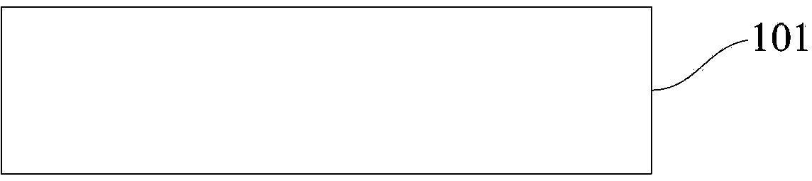
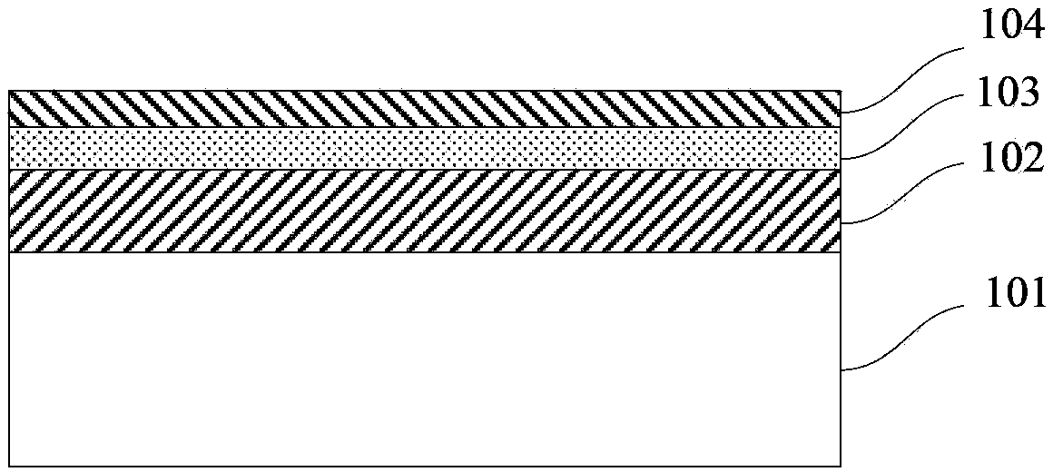
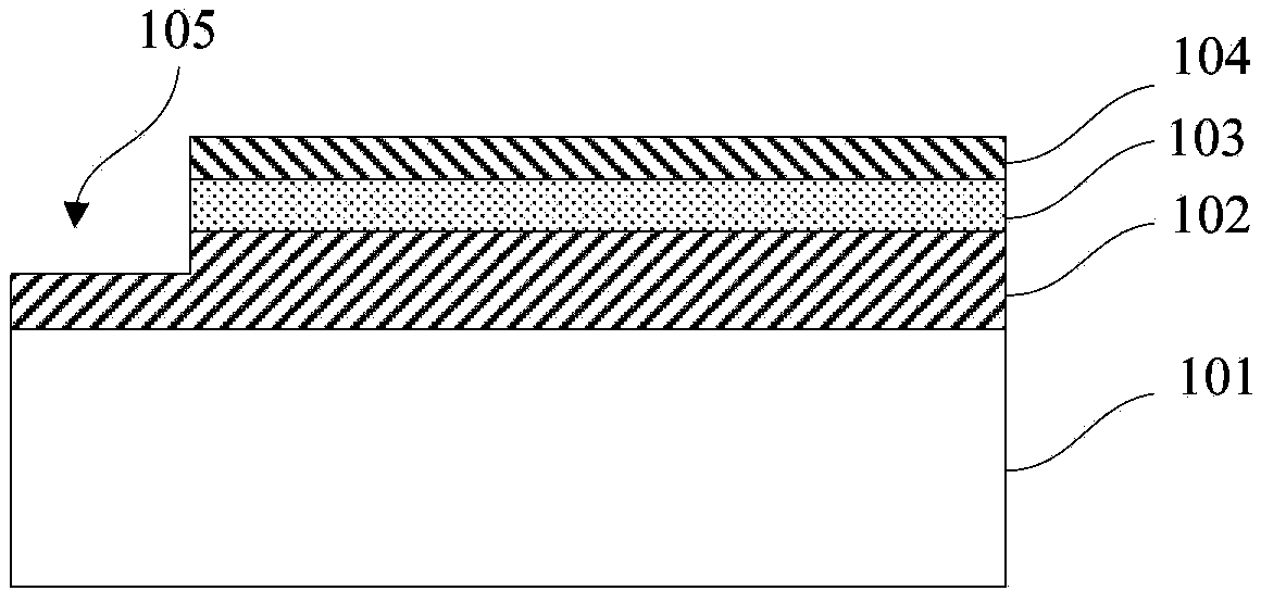
[0052] See Figure 1 ~ Figure 12 . It should be noted that the illustrations provided in this embodiment only illustrate the basic idea of ​​the present invention in a schematic way, and the figures only show the components related to the present invention instead of the number, shape, and shape of the components in actual implementation. For size drawing, the type, quantity, and proportion of each component can be changed at will during actu...


PUM

PropertyMeasurementUnit
Thicknessaaaaaaaaaa

Abstract

The invention provides a manufacturing method of a light emitting diode. The manufacturing method comprises the steps of 1) forming a light emitting epitaxy structure at least comprising an N-type layer, a quantum well layer and a P-type layer on the surface of a growth substrate, 2) forming a preparation area of an N electrode, 3) preparing a patterned structure on the surface of an area of the P-type layer for preparing a P electrode, 4) forming a metal reflector on the surface of the patterned structure, 5) forming a transparent insulating layer on the surface of the metal reflector, 6) forming a current spreading layer on the surfaces of the P-type layer and the transparent insulating layer, and 7) preparing the N electrode and the P electrode. According to the manufacturing method, a metal reflector / insulating layer structure is added below the P electrode, so that current is saved, and absorption of the P electrode to light is reduced greatly; the P-type layer below the metal reflector is coarsened, so that the light emitting probability is improved, and the firmness of the P electrode is facilitated; and the manufacturing method is simple in technology step, and is suitable for industrial production.

Description

Technical field [0001] The invention belongs to the field of semiconductor lighting, and particularly relates to a method for manufacturing a light emitting diode. Background technique [0002] As a new type of high-efficiency solid light source, semiconductor lighting has significant advantages such as long life, energy saving, environmental protection, and safety. It will become another leap in the history of human lighting after incandescent lamps and fluorescent lamps. Its application fields are rapidly expanding and are driving traditional lighting and display The economic and social benefits of the upgrading of other industries are huge. Because of this, semiconductor lighting is generally regarded as one of the most promising emerging industries in the 21st century, and one of the most important commanding heights in the optoelectronics field in the next few years. Light-emitting diodes are made of III-IV compounds, such as GaAs (gallium arsenide), GaP (gallium phosphide)...

Claims


Application Information

Patent Timeline
IPC IPC(8): H01L33/10H01L33/22
CPCH01L33/007H01L33/22H01L33/46
Inventor 朱广敏郝茂盛齐胜利陈耀张楠杨杰袁根如陈诚
Owner EPILIGHT TECH
Why Eureka
Try Eureka