Method for manufacturing shallow trench isolation structure

A technology of isolation structure and manufacturing method, which is applied in semiconductor/solid-state device manufacturing, electrical components, circuits, etc., and can solve problems such as the limitation of shallow trench isolation structure

Active Publication Date: 2017-06-13
GIGADEVICE SEMICON (BEIJING) INC
View PDF4 Cites 0 Cited by
  • Summary
  • Abstract
  • Description
  • Claims
  • Application Information

AI Technical Summary

Problems solved by technology

[0010] The main purpose of the present invention is to provide a method for manufacturing a shallow trench isolation structure, so as to solve the problem in the related art that the shallow trench isolation structure of a device with a process node of 65nm or below is limited by using KrF technology

Method used


Image

  • Method for manufacturing shallow trench isolation structure
  • Method for manufacturing shallow trench isolation structure
  • Method for manufacturing shallow trench isolation structure

Examples


Embodiment Construction

[0034] It should be noted that, in the case of no conflict, the embodiments in the present application and the features in the embodiments can be combined with each other. The present invention will be described in detail below with reference to the accompanying drawings and examples.

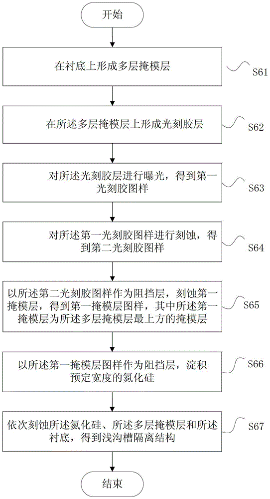
[0035] In an embodiment of the present invention, a method for manufacturing a shallow trench isolation structure is provided, image 3 is a flowchart of a method for manufacturing a shallow trench isolation structure according to an embodiment of the present invention. Such as image 3 As shown, the method includes:

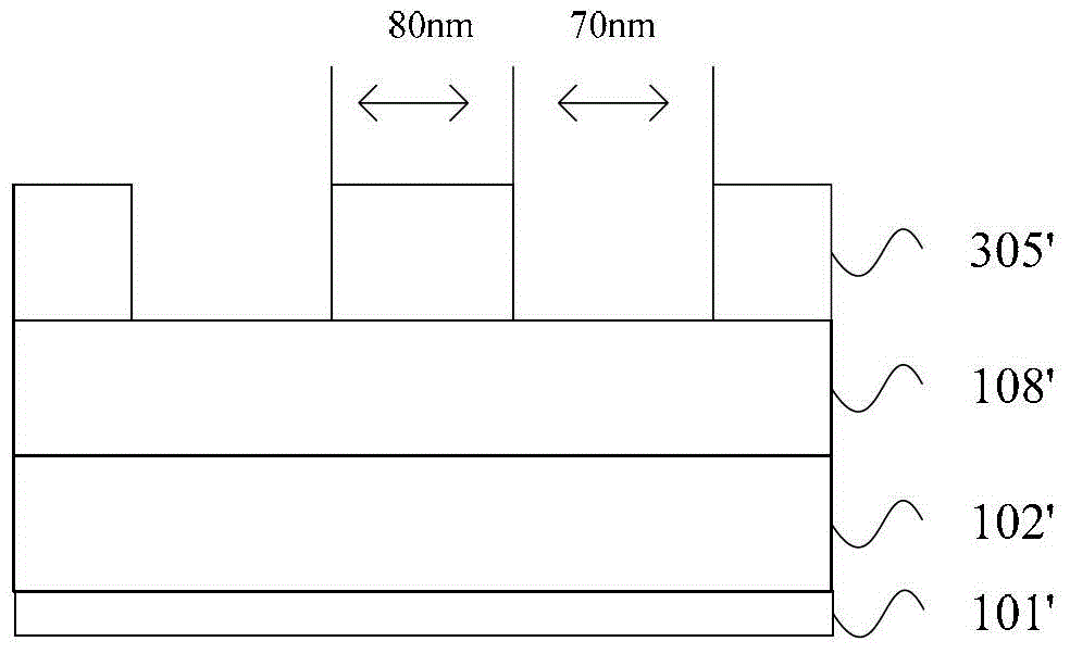
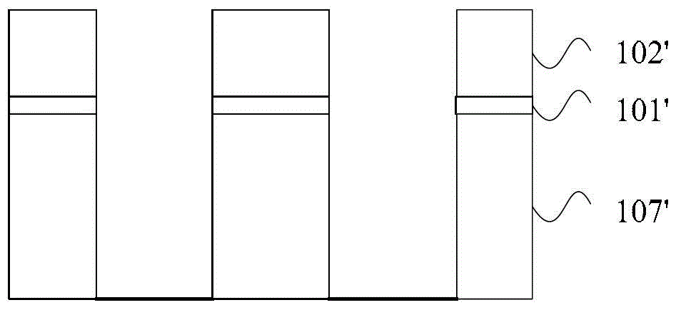
[0036] Step S61, forming a multi-layer mask layer on the substrate.

[0037] Step S62, forming a photoresist layer on the multi-layer mask layer.

[0038] Step S63, exposing the photoresist layer to obtain a first photoresist pattern.

[0039] Step S64, exposing the first photoresist pattern to obtain a second photoresist pattern.

[0040] Step S65, using the second photore...


PUM


Abstract

The invention discloses a fabrication method for a shallow trench isolation structure. The fabrication method for the shallow trench isolation structure comprises the following steps of: forming multiple mask layers on a substrate; forming a photoresist layer on the multiple mask layers; exposing the photoresist layer to obtain a first photoresist pattern; etching the first photoresist pattern to obtain a second photoresist pattern; etching a first mask layer by using the second photoresist pattern as a baffle layer to obtain a first mask layer pattern, wherein the first mask layer is a mask layer at the top of the multiple mask layers; depositing silicon nitride with a preset width by using the first mask layer pattern as the baffle layer; and sequentially the silicon nitride, the multiple mask layers and the substrate to obtain the shallow trench isolation structure. With the adoption of the fabrication method, the shallow trench isolation of a device with a process node of 65 nanometers or below 65 nanometers is fabricated on the condition of no adoption of an ArF photoetching machine.

Description

technical field [0001] The invention relates to the technical field of semiconductor manufacturing, in particular to a method for manufacturing a shallow trench isolation structure. Background technique [0002] With the advancement of science and technology, the semiconductor manufacturing process continues to develop, the size of the semiconductor device is continuously reduced, and the isolation structure of the semiconductor device is also reduced accordingly. An isolation structure between elements in an active area (abbreviated as AA) of a semiconductor device is usually formed by a shallow trench isolation (referred to as STI) process. [0003] The isolation structure of devices with a manufacturing process node size of 65nm or below mostly uses an ArF (wavelength 193nm) lithography machine. In the prior art, methods for forming shallow trench isolation structures generally include: [0004] 1) After depositing the active region isolation silicon nitride, a layer of ...

Claims


Application Information

Patent Timeline
Patent Type & Authority Patents(China)
IPC IPC(8): H01L21/762H01L21/027H01L21/033
CPCH01L21/0274H01L21/0332H01L21/76224
Inventor 于法波熊涛冯骏许毅胜吴楠
Owner GIGADEVICE SEMICON (BEIJING) INC
Why Eureka
Try Eureka