Trench isolation lateral insulated gate bipolar transistor

A bipolar transistor and trench isolation technology, applied in semiconductor devices, electrical components, circuits, etc., can solve the problems of unfavorable LIGBT device practical application, excessive device current density, current rebound, etc., and reduce current rebound. phenomenon, reduce the leakage current of the device, and improve the effect of the withstand voltage of the device

Active Publication Date: 2014-10-01
SOUTHEAST UNIV
View PDF5 Cites 2 Cited by
  • Summary
  • Abstract
  • Description
  • Claims
  • Application Information

AI Technical Summary

Problems solved by technology

However, RC-LIGBT has a very serious problem, that is, the current rebound phenomenon will occur during the forward conduction process of the device.
When multiple LIGBT devices are connected in parallel, if there is a phenomenon of current bounce in the device, it will cause the current density of a single device to be too high and burn out, which is not conducive to the practical application of LIGBT devices

Method used


Image

  • Trench isolation lateral insulated gate bipolar transistor
  • Trench isolation lateral insulated gate bipolar transistor
  • Trench isolation lateral insulated gate bipolar transistor

Examples


Embodiment Construction

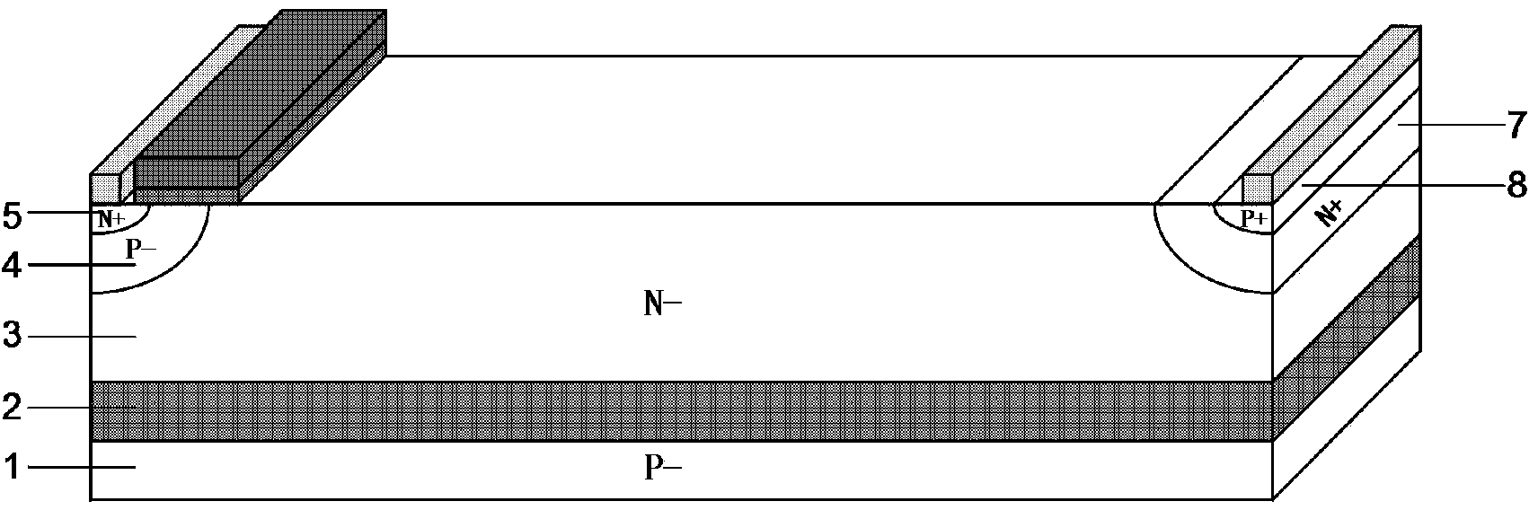
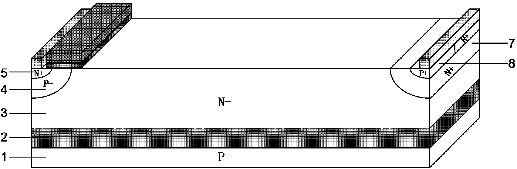
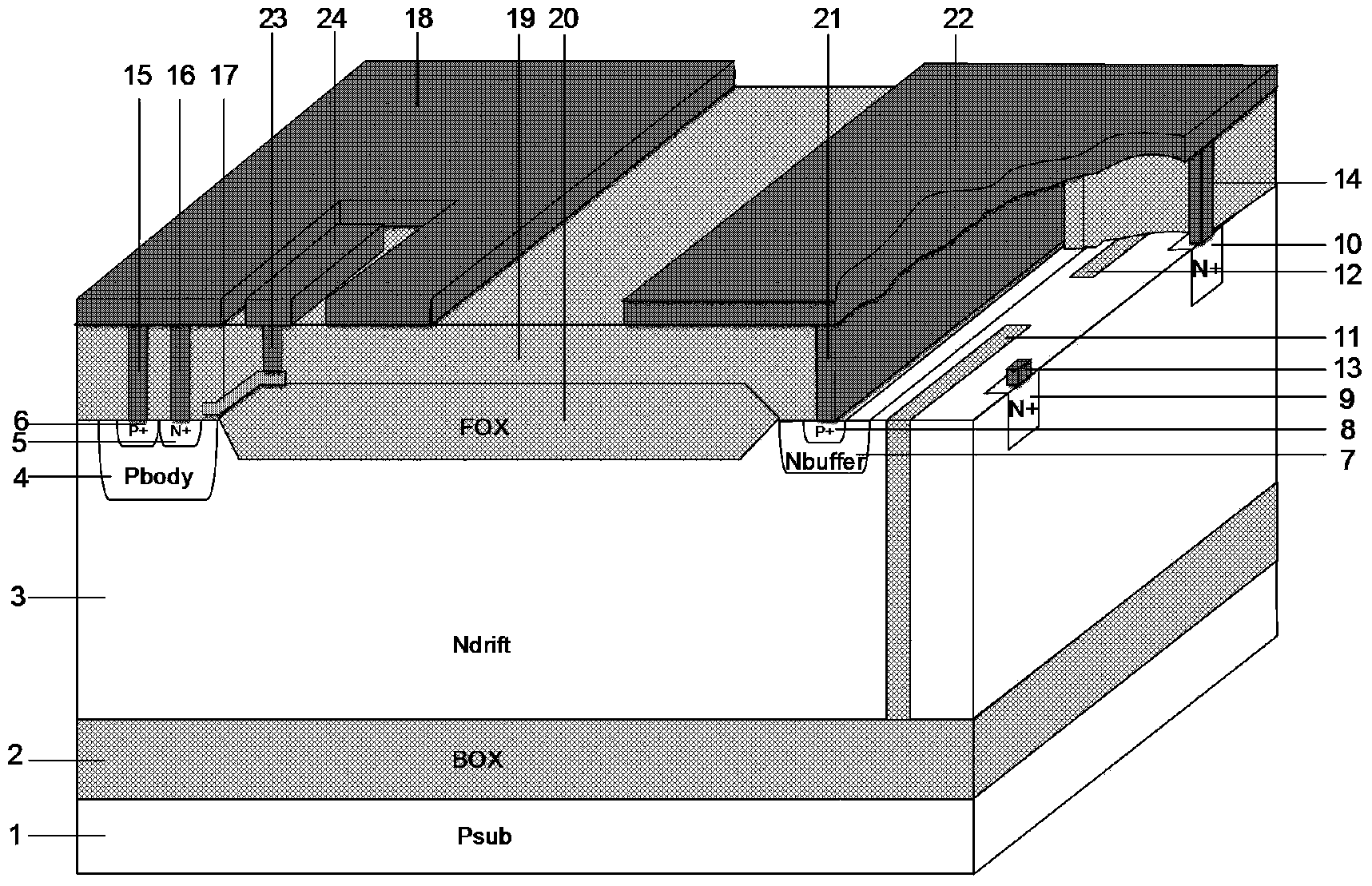
[0018] Combine below image 3 , the present invention is described in detail, a trench-isolated lateral insulated gate bipolar transistor, comprising: a P-type substrate 1 and a field oxide layer 20, a buried oxide 2 is arranged on the P-type substrate 1, and a buried oxide 2 A drift region 3 is provided on the upper surface, an oxide layer 19 is arranged above the upper surface of the drift region 3, a P-type body region 4 and an N-type buffer layer 7 are arranged below the upper surface of the drift region 3, and the field oxygen layer 20 Located between the P-type body region 4 and the N-type buffer layer 7 and between the drift region 3 and the oxide layer 19, the P-type body region 4 is provided with a connected P-type emitter region 6 and an N-type emitter region 5 A P-type collector region 8 is provided in the N-type buffer layer 7, a polysilicon gate 17 is provided in the oxide layer 19, and one end of the polysilicon gate 17 is located above the boundary of the N-type...


PUM


Abstract

The invention provides a semiconductor device capable of improving the voltage endurance capability and the high temperature endurance of a common insulated gate bipolar transistor and avoiding the current rebounding phenomenon. According to the semiconductor device, a P type substrate is provided with a buried oxide layer, the buried oxide layer is provided with a drift region, a P type body region is arranged on one side of the drift region, and an N type buffer layer is arranged on the other side of the drift region. A P type emitter region and an N type emitter region connected with the P type emitter region are arranged in the P type body region, and the P type body region is provided with metal used for being connected with the P type emitter region and the N type emitter region and an emitter metal field plate. A P type collector region is arranged in the N type buffer layer, and the N type buffer layer is provided with metal used for connection and a collector metal field plate. A polysilicon gate is arranged above the portion, between the buried oxide layer and the N type emitter region, of the P type body region. Two trench isolation layers are arranged outside an N type body region, a gap for a carrier to flow is reserved between the two trench isolation layers, and two N type collector regions are arranged outside the trench isolation layers and connected with the P type collector region through the metal.

Description

technical field [0001] The invention mainly relates to the technical field of power semiconductor devices, specifically, a trench-isolated lateral insulated gate bipolar transistor, which is especially suitable for high-power integrated circuits such as frequency conversion speed regulation, high-voltage power transmission, electric traction, frequency conversion household appliances, semi-conductors, etc. Bridge drive circuit and automobile production and other fields. Background technique [0002] Insulated Gate Bipolar Transistor IGBT is a composite power device evolved from the combination of MOS gate device structure and bipolar transistor structure. It has the characteristics of both MOS transistor and bipolar transistor, and has good on-state current and switching loss. compromise relationship between. Silicon-on-insulator lateral insulated gate bipolar transistor (SOI-Lateral Insulated Gate Bipolar Transistor, SOI-LIGBT) is a typical device based on SOI technology, ...

Claims


Application Information

Patent Timeline
IPC IPC(8): H01L29/739H01L29/06H01L29/40
CPCH01L29/0649H01L29/66325H01L29/7393
Inventor 孙伟锋杜益成喻慧张龙祝靖陆生礼时龙兴
Owner SOUTHEAST UNIV
Why Eureka
Try Eureka