Chip adaptive configuration method and device

A chip configuration, self-adaptive technology, applied in the direction of measuring devices, instruments, measuring electronics, etc., can solve the problems of increased material risk, unfavorable control of material cost, and narrowed range of material chips, so as to improve matching and reduce The effect of exclusive material risk and equipment stability improvement

Inactive Publication Date: 2014-09-03
ZTE CORP
View PDF6 Cites 3 Cited by
  • Summary
  • Abstract
  • Description
  • Claims
  • Application Information

AI Technical Summary

Problems solved by technology

In this way, it not only narrows the scope of using material chips, but also increases the risk of materials, and also has an adverse impact on the control of material costs.

Method used


Image

  • Chip adaptive configuration method and device
  • Chip adaptive configuration method and device
  • Chip adaptive configuration method and device

Examples


Embodiment Construction

[0048] The preferred embodiments of the present invention will be described in detail below in conjunction with the accompanying drawings. It should be understood that the preferred embodiments described below are only used to illustrate and explain the present invention, and are not intended to limit the present invention.

[0049] Figure 4 It is a flow chart of the method for adaptively configuring the chip provided by the present invention, such as Figure 4 As shown, the steps include:

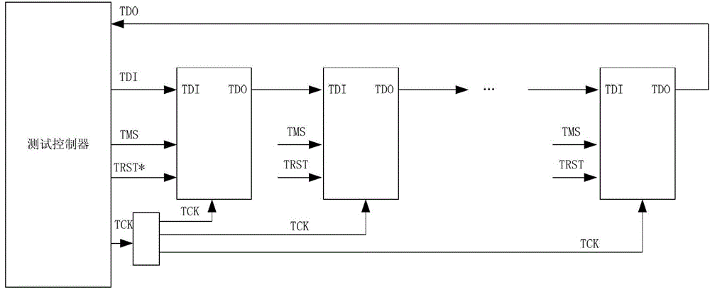
[0050] Step 401: when the chip is powered on, the test controller controls each chip to be identified to be in a scanning mode through a test link connected to each chip to be identified.

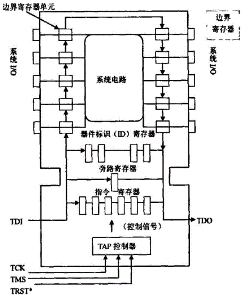
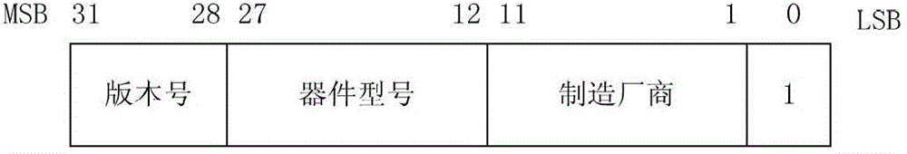
[0051] Step 402: The test controller scans the device identification register of each chip to be identified through the test link to identify and read out the chip model.

[0052] Step 403: After acquiring the chip model of each chip to be identified, the test controller controls the chip to be identif...


PUM


Abstract

The invention discloses a chip adaptive configuration method and device, and relates to the electronic equipment field; the method comprises the following steps: to connect each chip to be identified with a testing controller through a testing link; the testing controller scans each chip to be identified through the testing link so as to obtain a chip model of each chip to be identified; to determine configuration parameters of each chip to be identified and/or other chips connected with the chip to be identified according to the chip model of each chip to be identified, and to configure the configuration parameters to the corresponding chip. In a chip power-on process, device scanning is used to obtain the chip model of each chip to be identified, and the obtained chip model is used to carry out different configurations for the corresponding chip, thereby realizing best signal matching between interconnected chips.

Description

technical field [0001] The invention relates to the field of electronic equipment, in particular to a method for adaptively configuring a chip and a related device. Background technique [0002] Joint Test Action Group (JTAG) is an international standard test protocol (compatible with IEEE 1149.1), which is mainly used for internal testing of chips. Chips that support JTAG testing have a standard JTAG interface, and its 4 lines include: [0003] Clock line TCK - used for test clock input; [0004] Data input line TDI - used for testing data input, the data is input to the JTAG port of the chip through TDI; [0005] Data output line TDO - used for test data output, the data is output from the JTAG port of the chip through TDO; [0006] Mode selection line TMS - used for test mode selection, TMS is used to make the chip in a specific test mode through the JTAG port. [0007] Optional pin TRST - used for test reset, input pin, active low, used to make the chip enter and exi...

Claims


Application Information

Patent Timeline
Patent Type & Authority Applications(China)
IPC IPC(8): G01R31/3185
Inventor 罗伟
Owner ZTE CORP
Why Eureka
Try Eureka