A method for making ultra-thin odd-numbered-layer coreless board with low stress and low warpage

A low-warpage, odd-numbered layer technology, applied in multi-layer circuit manufacturing and other directions, can solve the problems of complex process, easy warpage, large warpage, etc., to simplify the preparation process, reduce mismatch, and reduce warpage. Effect

Active Publication Date: 2017-02-15
NAT CENT FOR ADVANCED PACKAGING
View PDF4 Cites 0 Cited by
  • Summary
  • Abstract
  • Description
  • Claims
  • Application Information

AI Technical Summary

Problems solved by technology

[0004] From the point of view of the above manufacturing process, the manufacturing method of this coreless board is to carry out substrate build-up processing on both sides of the carrier board at the same time, and odd-numbered layer substrates can be produced. However, due to the asymmetric structure of the odd-numbered layer substrates, the warpage is very large.
Even if an even-numbered substrate is used, since the laminated lamination method is only symmetrically distributed to the carrier board, when it is separated from the carrier board, there is no symmetrical center from the laminated section, and the lamination conditions of all layers are the same. There is a difference. Even if the material and thickness of the inner insulating layer and the outer layer are exactly the same, the high temperature process they experience is also very different, which leads to a large difference in the properties of the organic resin material itself, and the distribution of its internal stress. The difference is that it is difficult to eliminate the internal stress according to the conventional method. Therefore, regardless of the odd or even number of layers, it is inevitable that a large warpage will be generated inside the coreless board.
[0005] Therefore, the existing process for manufacturing Coreless substrates has problems such as complex process, easy warping, and difficult processing.

Method used


Image

  • A method for making ultra-thin odd-numbered-layer coreless board with low stress and low warpage
  • A method for making ultra-thin odd-numbered-layer coreless board with low stress and low warpage
  • A method for making ultra-thin odd-numbered-layer coreless board with low stress and low warpage

Examples


Embodiment Construction

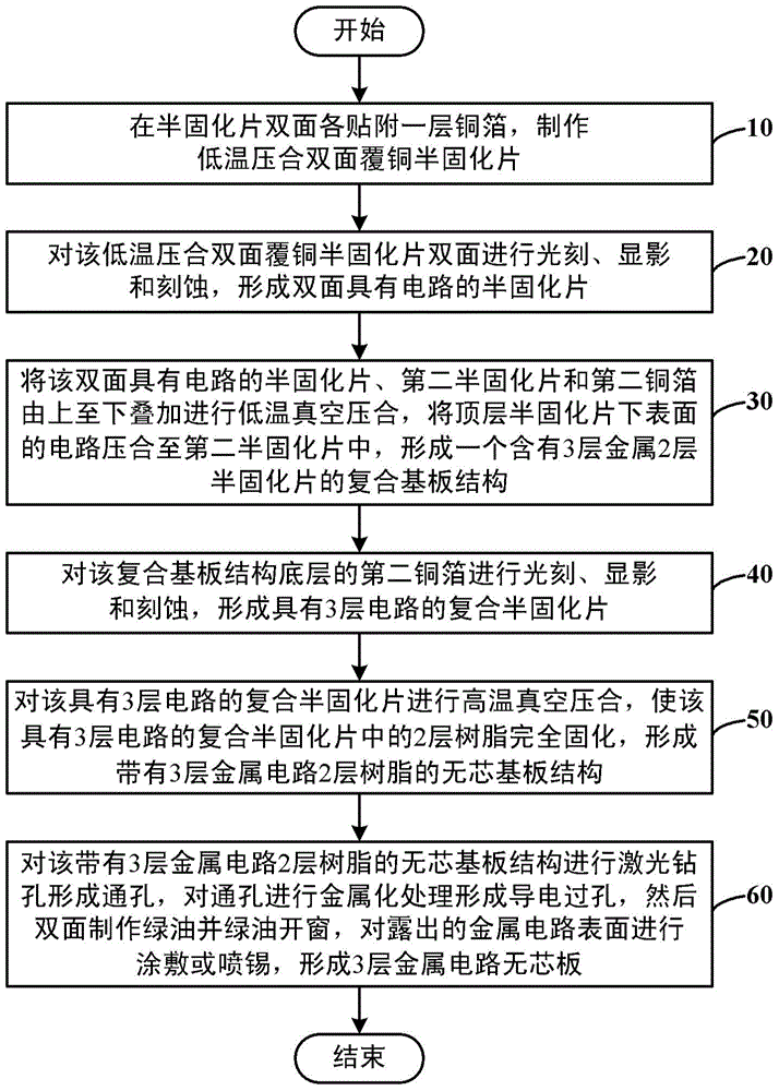
[0033] In order to make the object, technical solution and advantages of the present invention clearer, the present invention will be described in further detail below in conjunction with specific embodiments and with reference to the accompanying drawings.

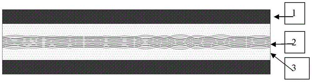
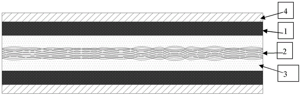
[0034] The present invention makes use of the characteristics of better resin fluidity of the prepreg at a certain low temperature, manufactures circuits on the surface of the prepreg at low temperature, and performs high-temperature vacuum lamination after manufacturing the three-layer circuit to form a three-layer circuit. Circuit board structure, two layers of prepreg are used in the three-layer circuit, and the high-temperature lamination conditions of the prepreg are exactly the same, and its structure is symmetrical with respect to the middle circuit layer, so, after lamination, its internal resin is relative to the middle The magnitude and direction of circuit stress can be compensated for each other, thus avoiding ...


PUM


Abstract

The invention discloses a method for manufacturing a low-stress low-warping-degree ultrathin odd-layer coreless plate. The method comprises the steps that two layers of copper foil are attached to the two sides of a semi-solidified sheet respectively, and a low-temperature press-fit two-side coppered semi-solidified sheet is manufactured; photoetching, developing and etching are carried out on the two sides of the two-side coppered semi-solidified sheet, and a semi-solidified sheet with circuits on the two sides is formed; the semi-solidified sheet, a second semi-solidified sheet and second copper foil are overlapped from top to bottom for low-temperature vacuum press fit, and a composite substrate structure is formed; photoetching, developing and etching are carried out on the second copper foil on the bottom layer of the composite substrate layer, and a composite semi-solidified sheet with three layers of circuits is formed; high temperature vacuum press fitting is carried out on the composite semi-solidified sheet to form a coreless substrate structure with three layers of metal circuits and two layers of resin; laser drilling is carried out on the coreless substrate structure to form through holes, metallization treatment is carried out on the through holes to form conductive via holes, green oil is manufactured on the two sides, the green oil is windowed, the surfaces of the exposed metal circuits are coated or sprayed with tin, and the three-layer metal circuit coreless plate is formed.

Description

technical field [0001] The invention relates to the technical field of coreless board manufacturing, in particular to a method for manufacturing an ultra-thin odd-numbered layer coreless board with low stress and low warpage. Background technique [0002] Coreless substrates are coreless substrates, which can make the package size thinner and smaller. It is currently a hot spot in the research and development of high-end substrates and has broad application prospects. [0003] Conventional Coreless substrates are coated with temporary bonding glue on both sides of a carrier board, and then make metal circuits layer by layer on the temporary bonding glue coated on both sides, and then separate the metal circuit structures on both sides of the carrier board from the carrier board to form Two coreless boards. [0004] From the point of view of the above-mentioned manufacturing process, the manufacturing method of this coreless board is to carry out substrate build-up processin...

Claims


Application Information

Patent Timeline
Patent Type & Authority Patents(China)
IPC IPC(8): H05K3/46
Inventor 于中尧
Owner NAT CENT FOR ADVANCED PACKAGING
Why Eureka
Try Eureka