
Preparation method for group I-III-VI tri-element semiconductor nanocrystalline light-emitting film

A light-emitting thin film and semiconductor technology, which is applied in the direction of semiconductor devices, light-emitting materials, chemical instruments and methods, etc., can solve the problems of particle agglomeration, volatilization, and increased difficulty, and achieve a wide coverage of fluorescence spectrum, simple synthesis equipment, and synthesis temperature mild effect

Active Publication Date: 2014-08-13
LIAONING UNIVERSITY
View PDF3 Cites 3 Cited by
  • Summary
  • Abstract
  • Description
  • Claims
  • Application Information

AI Technical Summary

Problems solved by technology

In order to solve the above problems, there are also studies on ternary semiconductor nanocrystal materials, but the existing problems are: first, the quantum efficiency of the synthesized semiconductor nanocrystal materials is low; second, the existing literature reports mostly by controlling the reaction conditions (temperature and Time) to adjust the fluorescence properties of semiconductor nanocrystals. The fluorescence range of the products obtained by this method is narrow, which is not enough to meet the requirements of practical applications. Third, the synthesized products are mostly stored in highly toxic solvents such as toluene and chloroform, which increases their application. Due to the difficulty of devices such as LEDs; Fourth, solvents such as toluene and chloroform are extremely volatile, resulting in particle agglomeration and greatly attenuating their fluorescence properties

Method used


Image

  • Preparation method for group I-III-VI tri-element semiconductor nanocrystalline light-emitting film
  • Preparation method for group I-III-VI tri-element semiconductor nanocrystalline light-emitting film
  • Preparation method for group I-III-VI tri-element semiconductor nanocrystalline light-emitting film

Examples


Embodiment 1

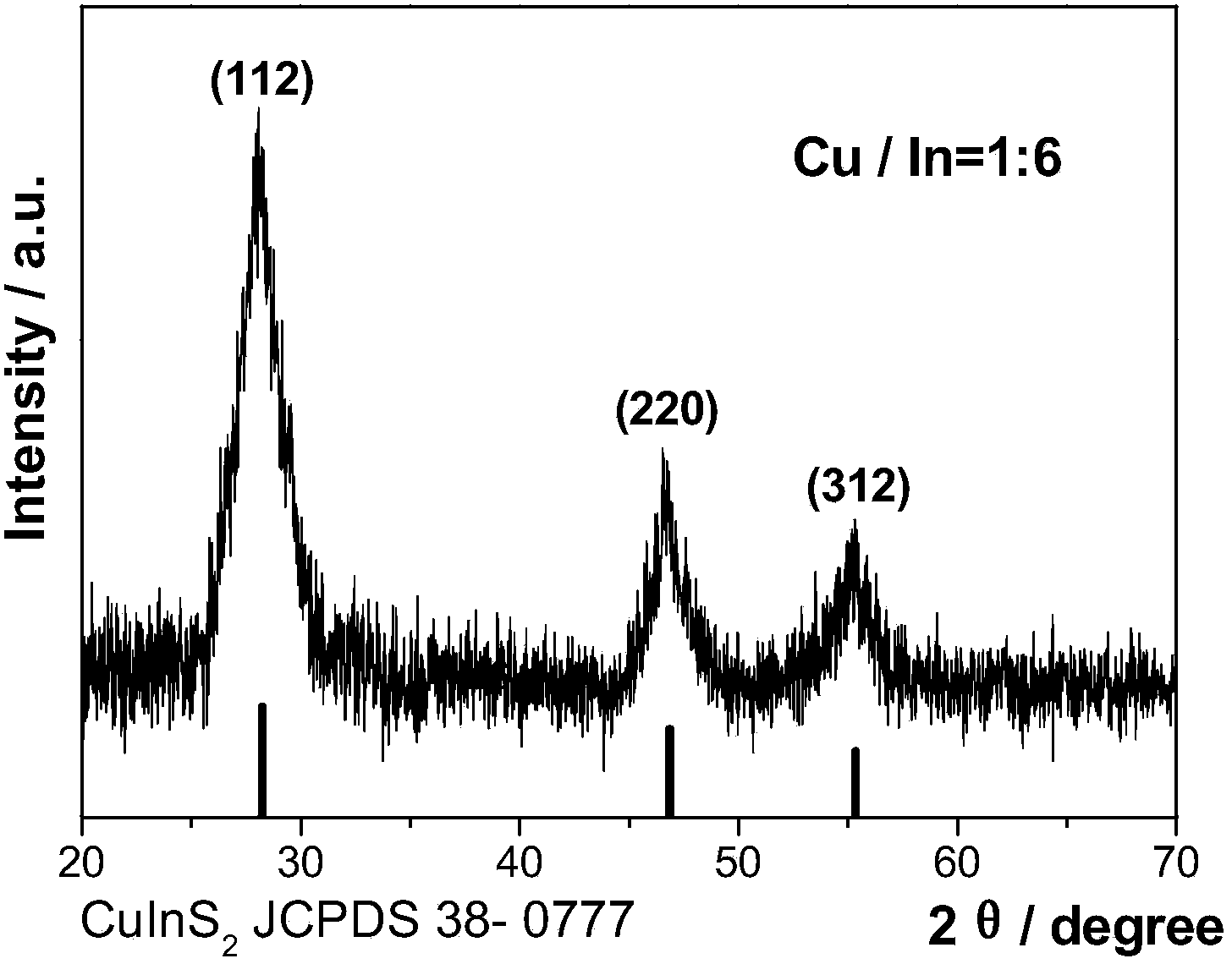
[0030] Example 1CuInS 2 Preparation method of ternary semiconductor nanocrystal luminescent film

[0031] In the first step, 9.9mg (0.1mmol) CuCl, 29.35mg (0.1mmol) InCl 3 4H 2 0, 2mmol n-dodecyl mercaptan, 0.2mmol oleic acid were added in the 8mL octadecene three-necked flask to obtain the mixed precursor solution; feed argon to get rid of the air, under the conditions of magnetic stirring and argon protection, Heat and mix the precursor solution to 180°C, under stirring, make CuCl, InCl 3 Dissolve completely until a pale yellow clear solution is formed.

[0032] In the second step, quickly inject 4 mL of sulfur in oleylamine solution into the light yellow clear solution (dissolve sulfur powder in oleylamine to make the sulfur concentration 0.2 mol / L). Adjust the temperature to 160°C, maintain the temperature, and let the reaction proceed for 90 minutes to prepare CuInS 2 Ternary semiconductor nanocrystal solution.

[0033] The third step, remove the heat source, make C...

Embodiment 2A

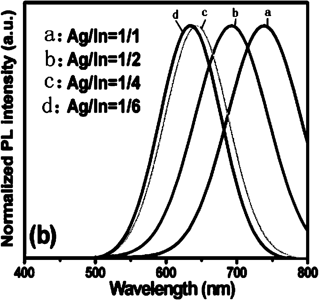
[0037] Example 2AgInS 2 Preparation method of ternary semiconductor nanocrystal luminescent film

[0038] In the first step, 16.9mg (0.1mmol) AgNO 3 , 29.35 mg (0.1 mmol) InCl 3 4H 2 0, 3mmol n-dodecyl mercaptan, 0.6mmol oleic acid were added in the 8mL octadecene three-necked flask, to obtain the mixed precursor solution; feed argon to get rid of the air, under the conditions of magnetic stirring and argon protection, Heat the mixed solution to 90°C and, under stirring, make the AgNO 3 , InCl 3 Dissolve completely until a pale yellow clear solution is formed.

[0039] In the second step, quickly inject 4mL sulfur oleylamine solution into the light yellow clear solution (dissolve sulfur powder in oleylamine to make the sulfur concentration 0.2mol / L), adjust the temperature to 110°C, and maintain the temperature, The reaction was carried out for 90min to prepare AgInS 2 Ternary semiconductor nanocrystal solution.

[0040] The third step, remove the heat source, make AgI...

Embodiment 3A

[0044] Example 3AgInS 2 Preparation method of ternary semiconductor nanocrystal luminescent film

[0045] In the first step, 16.9mg (0.1mmol) AgNO 3 , 58.7 mg (0.2 mmol) InCl 3 4H 2 0, 3mmol n-dodecyl mercaptan, 0.6mmol oleic acid were added in the 8mL octadecene three-necked flask, to obtain the mixed precursor solution; feed argon to get rid of the air, under the conditions of magnetic stirring and argon protection, Heat the mixed solution to 90°C and, under stirring, make the AgNO 3 , InCl 3 Dissolve completely until a pale yellow clear solution is formed.

[0046] In the second step, quickly inject 4mL sulfur oleylamine solution into the light yellow clear solution (dissolve sulfur powder in oleylamine to make the sulfur concentration 0.2mol / L), adjust the temperature to 110°C, and maintain the temperature, The reaction was carried out for 90min to prepare AgInS 2 Ternary semiconductor nanocrystal solution.

[0047] The third step, remove the heat source, make AgIn...


PUM

PropertyMeasurementUnit
quantum efficiencyaaaaaaaaaa

Abstract

The invention relates to a preparation method for a group I-III-VI tri-element semiconductor nanocrystalline light-emitting film. The employed technical scheme comprises: mixing a monovalent metal salt of group I elements, a trivalent chlorinated salt of group III elements, a capping agent, a surface coating agent and a nonpolar high-boiling-point solvent, so as to obtain a mixed precursor solution; under the protection of an inert gas, heating the mixed precursor solution from room temperature to 60-180 DEG C, so as to form a clear transparent solution; adding an oleylamine solution of a group VI element, so as to obtain a group I-III-VI tri-element semiconductor nanocrystalline solution; adding a polar solvent, performing centrifugation purifying; and then adding a composition A and a composition B of an LED pouring sealant, so as to obtain the group I-III-VI tri-element semiconductor nanocrystalline light-emitting film. The preparation process is green and environment-friendly, the preparation method is simple, and the prepared semiconductor nanocrystalline light-emitting film has excellent fluorescence performances of quantum dots and good machining performance of an epoxy resin AB glue substrate, and is applicable to solid-state lighting LED.

Description

technical field [0001] The invention relates to Ⅰ-Ⅲ-Ⅵ group ternary semiconductor nanocrystals (CuInS 2 , AgInS 2 etc.) The preparation of luminescent thin films belongs to the technical field of new fluorescent materials. Background technique [0002] The relatively mature II-VI and IV-VI semiconductor nanocrystals that have been studied so far contain heavy metal elements such as Cd and Pb, and are highly toxic. The preparation of semiconductor nanocrystals with low toxicity, wide luminescence range, adjustable luminescence peak position, high quantum efficiency (QY), and stable performance has become an urgent need for the synthesis of semiconductor nanocrystal materials. In order to solve the above problems, there are also studies on ternary semiconductor nanocrystal materials, but the existing problems are: first, the quantum efficiency of the synthesized semiconductor nanocrystal materials is low; second, the existing literature reports mostly control the reaction co...

Claims


Application Information

Patent Timeline
Patent Type & Authority Applications(China)
IPC IPC(8): C09K11/62H01L33/50
Inventor 李振荣陈兆平路亚群张忠利高宝禄邓胜龙
Owner LIAONING UNIVERSITY
Learn More