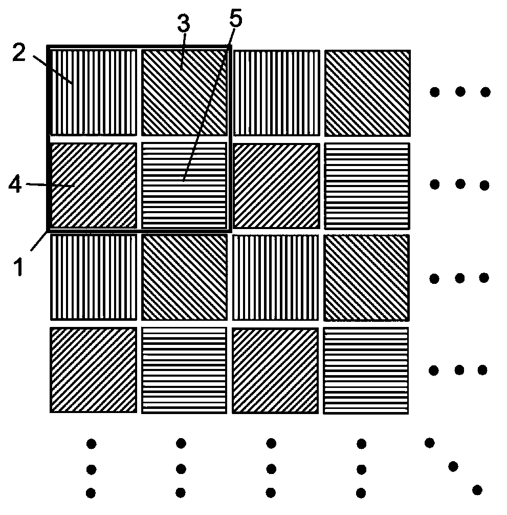
Micro polaroid array on basis of metal nanometer optical gratings and preparation method thereof
A technology of micro-polarizer array and metal nanometers, which is applied in the direction of polarizing elements, optical mechanical equipment, and photoplate-making process of pattern surface, etc., can solve the problems of increasing production cost, low transmittance, and reducing the consistency of process parameters, etc., to achieve The effect of reducing production costs and simplifying the process
- Summary
- Abstract
- Description
- Claims
- Application Information
AI Technical Summary
Problems solved by technology
Method used
Image
Examples
preparation example Construction
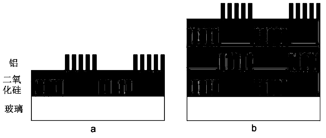
[0028] According to another aspect of the present invention, propose a kind of preparation method based on the single-layer micro-polarizer array of metal nano grating, such as Figure 4 Shown, this preparation method comprises the following steps:
[0029] Step 1. Carry out double-sided polishing and cleaning on the high-transmittance substrate. The substrate material is generally selected from materials with good transmission properties for light in the working band, such as glass or sapphire, and then electron beam deposition, chemical vapor deposition and The spin-coating method sequentially coats an aluminum layer, a silicon dioxide layer and a negative photoresist layer on the base material, wherein silicon dioxide is used as a hard template to etch the metal layer, such as Figure 4 as shown in a;
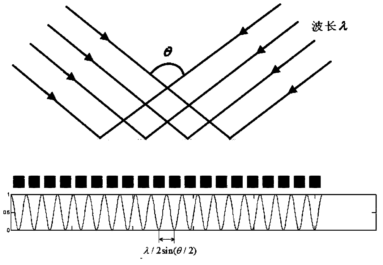
[0030] Step 2, use a laser to generate two beams of light for interference, and the generated interference fringes expose the photoresist, then turn off the interference li...
Embodiment 1
[0037] Embodiment 1, a micro-polarizer array with four polarization transmission directions was prepared according to the above method. The specific process is as follows:
[0038] Step 1. Using the glass substrate as the base material, optimize the glass surface through the mechanical chemical polishing (CMP) process, so that the fluctuation of the glass surface in the area of 3cm×3cm is within + / -5nm, and soak the glass sample in isopropanol and acetone in turn Cleaning, the sample is then placed in a reactive ion etching device, and further cleaned with oxygen by reactive ion etching, wherein the etching power is 300W, and the time is 20 minutes;
[0039] Step 2. Electron beam deposition and chemical vapor deposition are used to plate 140nm aluminum and 20nm silicon dioxide on the surface of the sample, and the silicon dioxide is used as a hard template to etch the aluminum layer;
[0040] Step 3. Spin-coat the negative photoresist onto the sample. The negative photoresi...
PUM
| Property | Measurement | Unit |
|---|---|---|
| thickness | aaaaa | aaaaa |
Abstract
Description
Claims
Application Information
 - R&D
- Intellectual Property
- Life Sciences
- Materials
- Tech Scout
- Unparalleled Data Quality
- Higher Quality Content
- 60% Fewer Hallucinations
Browse by: Latest US Patents, China's latest patents, Technical Efficacy Thesaurus, Application Domain, Technology Topic, Popular Technical Reports.
© 2025 PatSnap. All rights reserved.Legal|Privacy policy|Modern Slavery Act Transparency Statement|Sitemap|About US| Contact US: help@patsnap.com


