Method for inducting two-dimensional periodic structure on surface of material through femtosecond laser
A periodic structure, femtosecond laser technology, applied in the field of laser applications
- Summary
- Abstract
- Description
- Claims
- Application Information
AI Technical Summary
Problems solved by technology
Method used
Image
Examples
Embodiment 1
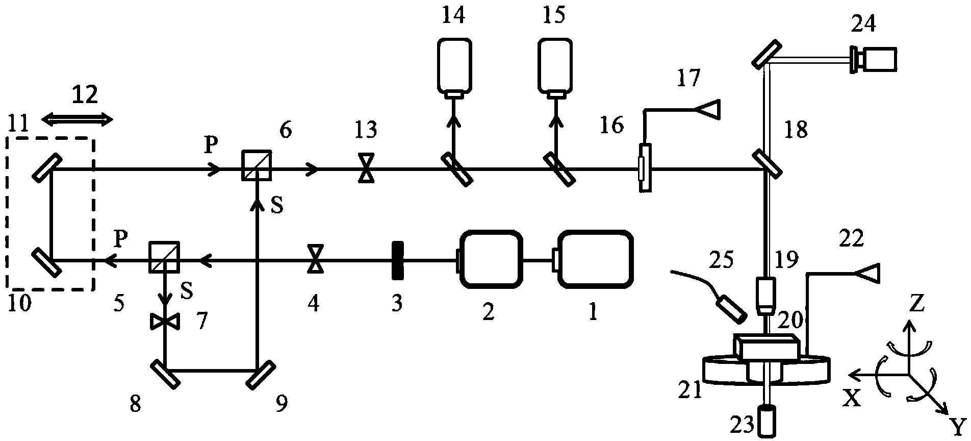
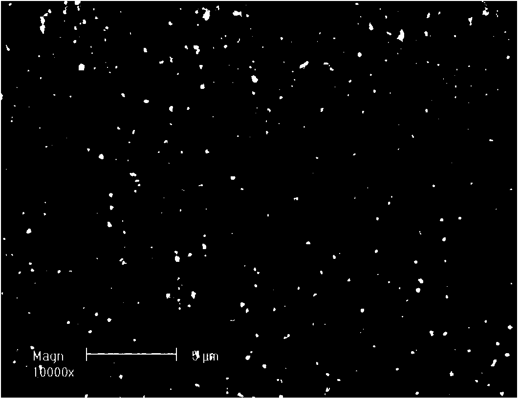
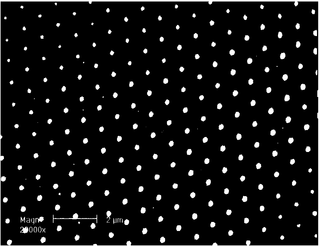
[0023] Taking the femtosecond laser variable wavelength vertical polarization double pulse processing method of the present invention to induce a two-dimensional periodic conical structure on the surface of Ge material as an example, the specific application equipment is as follows:
[0024] Femtosecond laser system 1 is a laser produced by Spectrum Physics in the United States. The laser wavelength is 800nm, the pulse width is 50fs, the repetition frequency is 1KHz, the maximum energy of a single pulse is 3mJ, and the light intensity distribution is Gaussian and linearly polarized.
[0025] The optical parametric amplifier 2 is TOPAS-C produced by American Light Conversion Company, which can continuously adjust the 800nm femtosecond laser pulse in the wavelength range of 290-2600nm with an adjustment accuracy of 0.1nm.
[0026] The structural components of the Michelson interferometer include: a polarization splitter prism 5 , a polarization combiner prism 6 , a first reflec...
Embodiment 2
[0034] The other steps are the same as in Embodiment 1, except that: in step (1), the laser wavelength is adjusted to 620nm through the optical parametric amplifier 2, wherein the wavelength adjustment accuracy is corrected by the fiber optic spectrometer 14; the period interval of the two-dimensional periodic conical structure becomes : 700-780nm.
Embodiment 3
[0036] The other steps are the same as in Example 1, except that: in step (1), the laser wavelength is adjusted to 1000 nm through the optical parametric amplifier 2, wherein the wavelength adjustment accuracy is corrected by the fiber optic spectrometer 14; the period interval of the two-dimensional periodic conical structure becomes : 1.1-1.25μm.
PUM
| Property | Measurement | Unit |
|---|---|---|
| radius | aaaaa | aaaaa |
| diameter | aaaaa | aaaaa |
| height | aaaaa | aaaaa |
Abstract
Description
Claims
Application Information
 - Generate Ideas
- Intellectual Property
- Life Sciences
- Materials
- Tech Scout
- Unparalleled Data Quality
- Higher Quality Content
- 60% Fewer Hallucinations
Browse by: Latest US Patents, China's latest patents, Technical Efficacy Thesaurus, Application Domain, Technology Topic, Popular Technical Reports.
© 2025 PatSnap. All rights reserved.Legal|Privacy policy|Modern Slavery Act Transparency Statement|Sitemap|About US| Contact US: help@patsnap.com


