Two-color all-optical switch based on cavity-induced coherence effect of quantum well intersubband transition
A coherent effect, all-optical switching technology, applied in electrical components, circuits, semiconductor devices, etc., can solve the problems of large resonant cavity size and difficult integration, achieve low energy consumption, easy miniaturization and integration, and achieve miniaturization and integration. integrated effect
- Summary
- Abstract
- Description
- Claims
- Application Information
AI Technical Summary
Problems solved by technology
Method used
Image
Examples
Embodiment 1
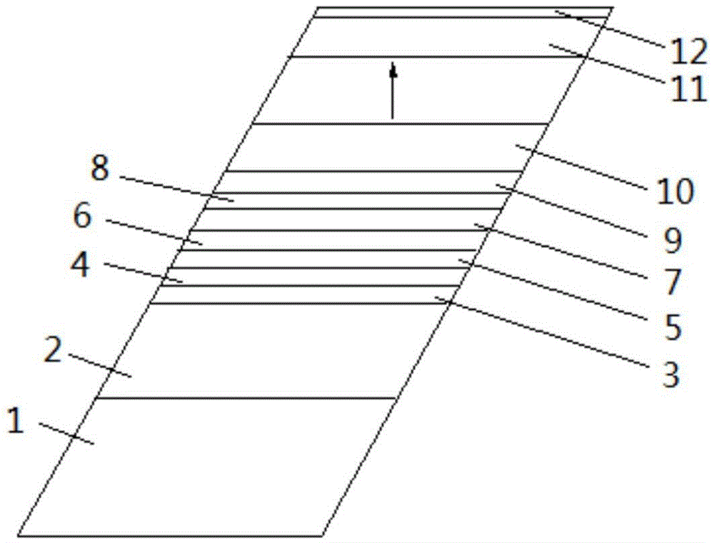
[0020] refer to figure 1 , the substrate 1 is GaAs, followed by an AlAs layer with a thickness of 3900nm; the first barrier layer 3 is composed of Al 0.4 Ga 0.6 As, the thickness is 20nm; the first quantum well layer 4, the composition is Al 0.16 Ga 0.84 As, the thickness is 6.7nm; the second barrier layer 5, the composition is Al 0.4 Ga 0.6 As, the thickness is 4.2nm; the second quantum well layer 6, the composition is Al 0.16 Ga 0.84 As, the thickness is 6.7nm; the third barrier layer 7, the composition is Al 0.4 Ga 0.6 As, with a thickness of 4.2nm; the third quantum well layer 8, composed of GaAs, with a thickness of 7.8nm; the fourth barrier layer 9, composed of Al 0.4 Ga 0.6 As, the thickness is 2.9nm; the continuum 10, the composition is Al 0.16 Ga 0.84 As, the thickness is 160nm. From the first barrier layer 3 to the continuous region 10 is a cycle, and then grow 9 cycles, a total of 10 cycles, and then grow a cover layer 11, the composition is Al 0.4 Ga ...
Embodiment 2
[0022] refer to figure 1 , the substrate 1 is GaAs, followed by an AlAs layer with a thickness of 5000nm; the first barrier layer 3 is composed of Al 0.35 Ga 0.65 As, the thickness is 10nm; the first quantum well layer 4, the composition is Al 0.1 Ga 0.9 As, the thickness is 8nm; the second barrier layer 5, the composition is Al 0.35 Ga 0.65 As, the thickness is 3nm; the second quantum well layer 6, the composition is Al 0.1 Ga 0.9 As, the thickness is 8nm; the third barrier layer 7, the composition is Al 0.35 Ga 0.65 As, the thickness is 3nm; the third quantum well layer 8 is composed of GaAs, and the thickness is 10nm; the fourth barrier layer 9 is composed of Al 0.35 Ga 0.65 As, the thickness is 2nm; the continuum 10, the composition is Al 0.1 Ga 0.9 As, the thickness is 160nm. From the first barrier layer 3 to the continuous region 10 is a cycle, and then grow 14 cycles, a total of 15 cycles, and then grow a cover layer 11, the composition is Al 0.4 Ga 0.6 A...
Embodiment 3
[0024] refer to figure 1 , the substrate 1 is GaAs, followed by an AlAs layer with a thickness of 2000nm; the first barrier layer 3 is composed of Al 04 Ga 0.6 As, the thickness is 30nm; the first quantum well layer 4, the composition is Al 0.2 Ga 0.8 As, the thickness is 1.8nm; the second barrier layer 5, the composition is Al 04 Ga 0.6 As, the thickness is 5nm; the second quantum well layer 6, the composition is Al 0.2 Ga 0.8 As, the thickness is 1.8nm; the third barrier layer 7, the composition is Al 04 Ga 0.6 As, the thickness is 5nm; the third quantum well layer 8 is composed of GaAs, and the thickness is 5.3nm; the fourth barrier layer 9 is composed of Al 04 Ga 0.6 As, the thickness is 4.5nm; the continuum 10, the composition is Al 0.2 Ga 0.8 As, the thickness is 160nm. From the first barrier layer 3 to the continuous region 10 is a period, and then grow 5 periods, a total of 6 periods, and then grow a covering layer 11, the composition is Al 0.4 Ga 0.6 As...
PUM
 Abstract
Description
Claims
Application Information
 - R&D
- Intellectual Property
- Life Sciences
- Materials
- Tech Scout
- Unparalleled Data Quality
- Higher Quality Content
- 60% Fewer Hallucinations
Browse by: Latest US Patents, China's latest patents, Technical Efficacy Thesaurus, Application Domain, Technology Topic, Popular Technical Reports.
© 2025 PatSnap. All rights reserved.Legal|Privacy policy|Modern Slavery Act Transparency Statement|Sitemap|About US| Contact US: help@patsnap.com


