
Printed circuit board buried resistor machining method

A technology of printed circuit boards and processing methods, which is applied in the direction of containing printed electrical components and removing conductive materials by chemical/electrolytic methods, which can solve the problem of affecting wiring density, wasting materials, and the accuracy and consistency can only be controlled within 25 % and other problems, to achieve high precision and consistency, improve wiring density, and high precision

Active Publication Date: 2014-07-02
SHANGHAI MEADVILLE SCI & TECH +1
View PDF5 Cites 8 Cited by
  • Summary
  • Abstract
  • Description
  • Claims
  • Application Information

AI Technical Summary

Problems solved by technology

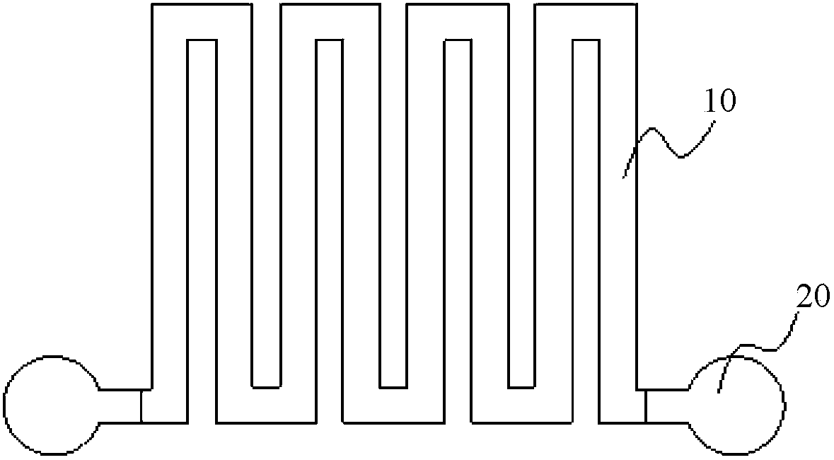
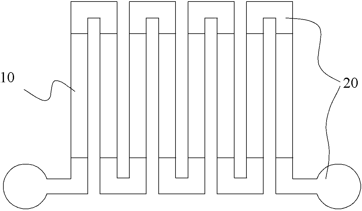
The length and width of the resistance formed by the etching method are formed by etching. The precision of the length and width of the resistance depends on the etching process. The conventional etching process is affected by the etching equipment, potion, and the exchange of the etching potion on the board during the etching process. Influenced by the impact of the resistance, its accuracy and consistency can only be controlled within 25%, which is difficult to meet the needs of high-precision resistance processing; or in order to achieve high-precision requirements, the width of the resistance needs to be designed very wide, which not only wastes materials, but also Affects Routing Density

Method used


Image

  • Printed circuit board buried resistor machining method
  • Printed circuit board buried resistor machining method
  • Printed circuit board buried resistor machining method

Examples


Embodiment Construction

[0083] The present invention will be further described below in conjunction with the accompanying drawings and embodiments.

[0084] see Figure 10 ~ Figure 18 , an embodiment of the method for processing buried resistors in printed circuit boards of the present invention, which adopts a material with a square resistance of 50 ohms, and processes a target resistance of 250 ohms.

[0085] The resistance value of the resistor is calculated by the following formula (I):

[0086] R=(b / a)×R S (I)

[0087] Among them; R S =ρ / H, the resistance width a is set to 100 μm, then the resistance etching length b is 250 / 50×100=500 μm.

[0088] Specific steps are as follows:

[0089] 1) Resistance copper foil lamination

[0090] The 50 ohm square resistance, the resistance copper foil 2 containing the resistance layer material 1, and the dielectric material 3 are pressed onto the substrate 8 on which the circuit pattern has been made, and the resistance layer material 1 is formed be...


PUM

PropertyMeasurementUnit
Surface roughnessaaaaaaaaaa

Abstract

The invention provides a printed circuit board buried resistor machining method. The method comprises the following steps: 1) the resistor copper coil pressing process is performed; 2) the thinning process is performed; 3) the anti-plating pattern fabrication process is performed; 4) the circuit pattern plating process is performed; 5) the film removing process is performed; 6) the circuit pattern etching process is performed, that is the first etching; 7) the resistor layer material exposing etching process is performed, that is the second etching; 8) the resistor pattern fabrication process is performed, that is the third etching; 9) the subsequent fabrication process of the printed circuit board is completed according to a conventional PCB method to finally obtain a printed circuit board having a buried resistor having advantages of high accuracy and high consistency. According to the invention, the buried resistor in the printed circuit board is fabricated by adopting the improved semi-additive process, so the resistance value accuracy and consistency of the buried resistor can be improved effectively, and especially the accuracy and consistency of a small-size buried resistor in the printed circuit board can be improved. The method of the invention is suitable for the machining of the buried resistor in the printed circuit board, and especially the printed circuit board having high small-size, high resistance value accuracy and high consistency requirements.

Description

technical field [0001] The invention relates to a processing method of a printed circuit board, in particular to a processing method of a buried resistor in a printed circuit board, which uses an improved semi-additive process to manufacture the buried resistor in the printed circuit board, and the processing method can effectively Improve the precision and consistency of the resistance value of buried resistors, especially for improving the precision and consistency of small-sized resistors buried in printed circuit boards. The invention is applicable to the processing of embedded resistors in printed circuit boards (PCB), especially for printed circuit boards with small size, high requirements on resistance precision and consistency. Background technique [0002] With the development of electronic products in the direction of lightness, thinness, shortness, smallness, multi-function, modularization, and integration, printed circuit boards (PCBs) as mounting components also...

Claims


Application Information

Patent Timeline
IPC IPC(8): H05K3/06H05K1/16
Inventor 罗永红吴金华陈培峰付海涛张坤黄伟
Owner SHANGHAI MEADVILLE SCI & TECH
Learn More