Glass composition for semiconductor junction protection, method for manufacturing semiconductor device, and semiconductor device
A technology of glass composites and manufacturing methods, which is applied in the direction of semiconductor/solid-state device manufacturing, semiconductor devices, semiconductor/solid-state device components, etc., to achieve the effect of reducing bending
- Summary
- Abstract
- Description
- Claims
- Application Information
AI Technical Summary
Problems solved by technology
Method used
Image
Examples
Embodiment approach 1
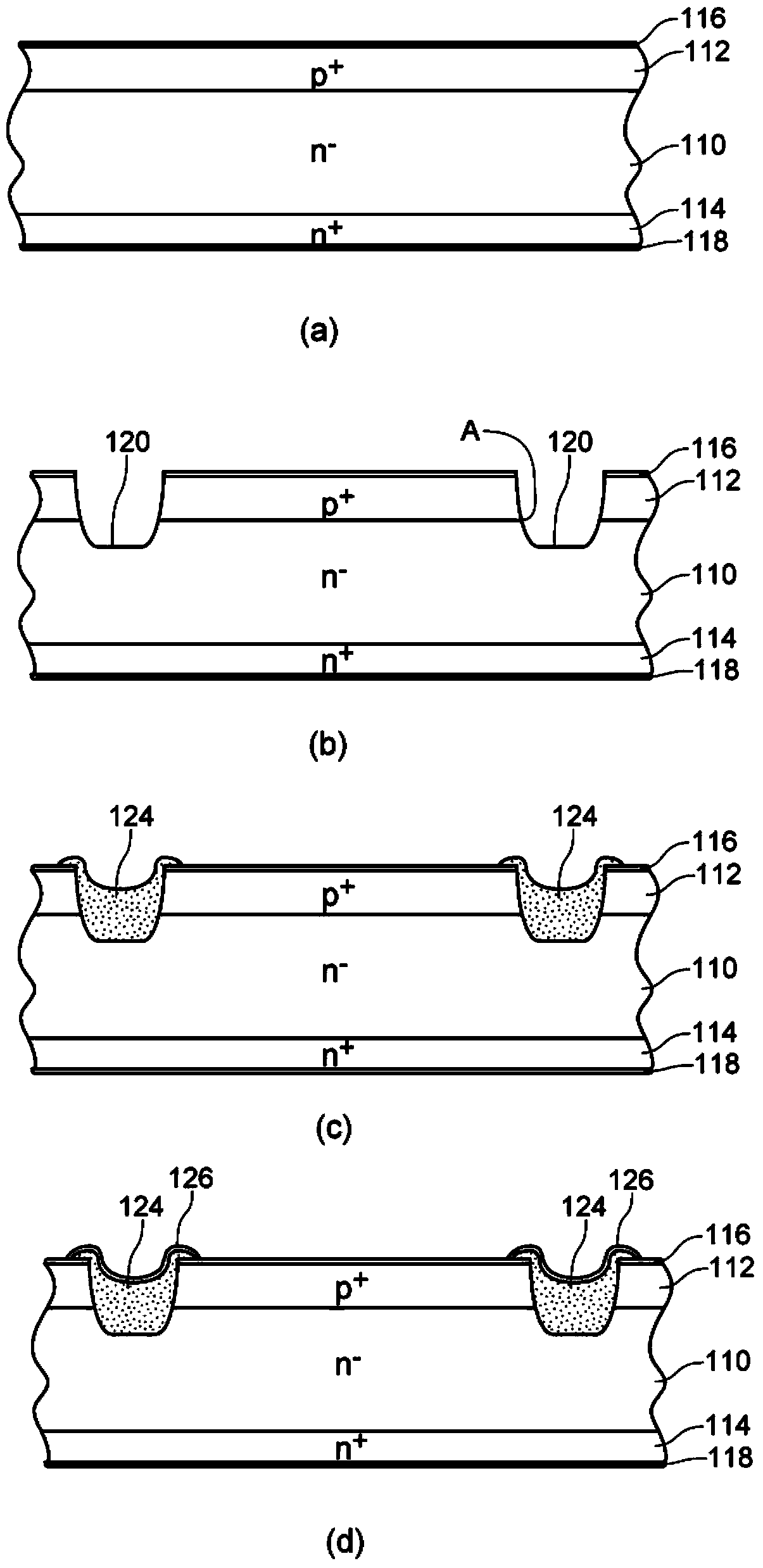
[0076] Embodiment 1 is an embodiment related to the glass compound for semiconductor junction protection.
[0077] The glass compound for semiconductor junction protection according to Embodiment 1 contains at least SiO 2 , B 2 o 3 , Al 2 o 3 , ZnO, and all alkaline earth metal oxides in CaO, MgO, and BaO, as well as nickel oxides, and substantially does not contain Pb, As, Sb, Li, Na, K. In this case, the inclusion of a certain specific component includes not only the case of containing only the certain specific component, but also the case of containing components that may be generally contained in glass composites in addition to the certain specific component. In addition, substantially not containing a certain specific element means that the certain specific element is not contained as a component, but glass composites in which the above-mentioned certain specific element is mixed as an impurity in the raw materials of each component constituting the glass are not excl...
Embodiment approach 2
[0094] Embodiment 2 is an embodiment related to the glass compound for semiconductor junction protection.
[0095] The glass compound for semiconductor junction protection according to Embodiment 2 contains at least SiO 2 , B 2 o 3 , Al 2 o 3 , ZnO, at least two alkaline earth metal oxides (CaO and BaO), and nickel oxide, and substantially free of Pb, As, Sb, Li, Na, K. In this case, the inclusion of a certain specific component includes not only the case of containing only the certain specific component, but also the case of containing components that may be generally contained in glass composites in addition to the certain specific component. In addition, substantially not containing a certain specific element means that the certain specific element is not contained as a component, but glass composites in which the above-mentioned certain specific element is mixed as an impurity in the raw materials of each component constituting the glass are not excluded. In addition,...
Embodiment approach 3
[0105] Embodiment 3 is an embodiment related to a glass compound for semiconductor junction protection.
[0106] The glass compound for protecting a semiconductor junction according to the third embodiment basically contains the same components as the glass compound for protecting a semiconductor junction according to the first embodiment, but is different from the semiconductor junction according to the first embodiment in that it does not contain nickel oxide. The protective glass compound is different. That is, the glass compound for semiconductor junction protection according to Embodiment 3 contains at least SiO 2 , B 2 o 3 , Al 2 o 3 , ZnO, and all alkaline earth metal oxides in CaO, MgO and BaO, and substantially do not contain Pb, As, Sb, Li, Na, K. In this case, the inclusion of a certain specific component includes not only the case of containing only the certain specific component, but also the case of containing components that may be generally contained in gl...
PUM
| Property | Measurement | Unit |
|---|---|---|
| Thickness | aaaaa | aaaaa |
Abstract
Description
Claims
Application Information
 - R&D
- Intellectual Property
- Life Sciences
- Materials
- Tech Scout
- Unparalleled Data Quality
- Higher Quality Content
- 60% Fewer Hallucinations
Browse by: Latest US Patents, China's latest patents, Technical Efficacy Thesaurus, Application Domain, Technology Topic, Popular Technical Reports.
© 2025 PatSnap. All rights reserved.Legal|Privacy policy|Modern Slavery Act Transparency Statement|Sitemap|About US| Contact US: help@patsnap.com


