
Miniaturized substrate integrated waveguide based on metamaterial

A substrate-integrated waveguide and super-medium technology, applied in waveguides, waveguide-type devices, circuits, etc., can solve the problems of limited design and narrow bandwidth, and achieve the effects of reduced lateral electrical dimensions, ease of processing, and deterioration of transmission coefficients

Inactive Publication Date: 2014-06-25
HARBIN INST OF TECH
View PDF2 Cites 9 Cited by
  • Summary
  • Abstract
  • Description
  • Claims
  • Application Information

AI Technical Summary

Problems solved by technology

[0004] Yuan Dang Dong et al. proposed to etch a complementary resonant ring (CSRR) on the upper surface of the substrate integrated waveguide to design a miniaturized narrowband filter, and finally obtained a narrowband frequency band below the cutoff frequency. However, since the CSRR is a resonant structure, the narrowband The bandwidth is very narrow, the relative bandwidth is only about 6%, which limits its use in the design of broadband devices
Then on this basis, they proposed a substrate-integrated waveguide based on a transmission line structure, but there is still a shortcoming that the bandwidth is too narrow, and the relative bandwidth is only 6.5%.

Method used


Image

  • Miniaturized substrate integrated waveguide based on metamaterial
  • Miniaturized substrate integrated waveguide based on metamaterial
  • Miniaturized substrate integrated waveguide based on metamaterial

Examples


specific Embodiment approach 1

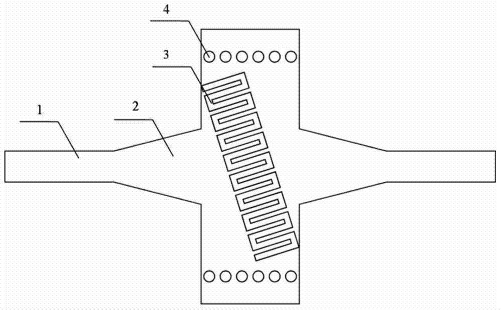
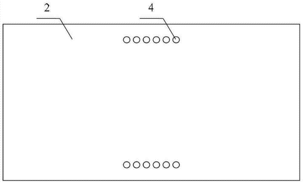
[0025] Specific implementation mode 1. Combination Figures 1 to 3 Illustrate this specific embodiment, the miniaturized substrate integrated waveguide based on supernormal medium, it comprises substrate and dielectric plate, and described substrate is fixed below the dielectric plate; It comprises two 50Ω microstrip lines 1 and two microstrip lines and Substrate-integrated waveguide conversion structure 2;

[0026] Each 50Ω microstrip line 1 is a metal strip structure; each microstrip line and substrate integrated waveguide conversion structure 2 is a gradually widening metal strip;

[0027] The two microstrip lines and the wider end of the substrate-integrated waveguide conversion structure 2 are mirrored and fixed in the middle of the left and right sides of the dielectric plate;

[0028] One end of the two 50Ω microstrip lines 1 is respectively connected to the narrower end of the two microstrip lines and the substrate-integrated waveguide conversion structure 2 as an int...

specific Embodiment approach 2

[0045] Embodiment 2. The difference between this embodiment and the miniaturized substrate-integrated waveguide based on meta-media described in Embodiment 1 is that the dielectric constant of the printed circuit board is 2.2.

specific Embodiment approach 3

[0046] Embodiment 3. The difference between this embodiment and the miniaturized substrate-integrated waveguide based on meta-media described in Embodiment 1 lies in the distance between the interdigitated capacitance slot (3) and the central axis of the printed circuit board. The included angle is between 0 degrees and 17.5 degrees.


PUM

PropertyMeasurementUnit
Reflection coefficientaaaaaaaaaa

Abstract

The invention relates to a miniaturized substrate integrated waveguide based on a metamaterial and aims at achieving integrated waveguide miniaturization under the condition that the working band width is ensured. The miniaturized substrate integrated waveguide comprises two 50omega microstrip lines and two microstrip line and substrate integrated waveguide conversion structures. each 50omega microstrip line is of a metal strip structure. Each microstrip line and substrate integrated waveguide conversion structure is a gradually wide metal strip. Wide-end mirror images of the microstrip line and substrate integrated waveguide conversion structures are fixed at the middle positions of the left and right sides of a dielectric slab. One end of each of two omega microstrip lines is respectively connected with the narrow ends of the microstrip line and substrate integrated waveguide conversion structures to form an integral structure. The upper portion and the lower portion of the dielectric slab are correspondingly provided with 2N metal through holes. Interdigital capacitor slots are etched between the through holes at the upper portion and the lower portion of the dielectric slab. The miniaturized substrate integrated waveguide serves as an integrated waveguide device.

Description

technical field [0001] The invention relates to a substrate integrated waveguide based on a supernormal medium. Background technique [0002] In recent years, Wu Ke and other scholars proposed a new type of low-profile substrate-integrated waveguide (SIW). The substrate-integrated waveguide is a new type of microwave transmission line, which is realized by reasonably laying two rows of metal vias on both sides of the printed circuit board (PCB). Utilizing this technology can not only reduce the size, weight and cost of traditional waveguides, but also greatly improve the feasibility and reliability of processing, so it is beneficial to produce integrated waveguide devices, especially when combined with supernormal media, it can design Better waveguide devices. [0003] Supernormal media are artificially designed special structures with abnormal electromagnetic properties. Due to their abnormal electromagnetic properties, they have received extensive attention in the microw...

Claims


Application Information

Patent Timeline
IPC IPC(8): H01P3/08
Inventor 傅佳辉沃得良张狂
Owner HARBIN INST OF TECH
Learn More