Photoelectric detector of spatial modulation structure and preparation method thereof

A photodetector and spatial modulation technology, applied in the direction of electric solid-state devices, circuits, electrical components, etc., can solve the problems of inability to realize full differential signal output, and achieve the elimination of smearing effect, reduction of transit time, and good performance Effect

Inactive Publication Date: 2014-05-07
TIANJIN UNIV
View PDF6 Cites 10 Cited by
  • Summary
  • Abstract
  • Description
  • Claims
  • Application Information

AI Technical Summary

Problems solved by technology

However, the above-mentioned detector is a pseudo-differential structure, which cannot realize full differential signal output

Method used


Image

  • Photoelectric detector of spatial modulation structure and preparation method thereof
  • Photoelectric detector of spatial modulation structure and preparation method thereof
  • Photoelectric detector of spatial modulation structure and preparation method thereof

Examples


Embodiment Construction

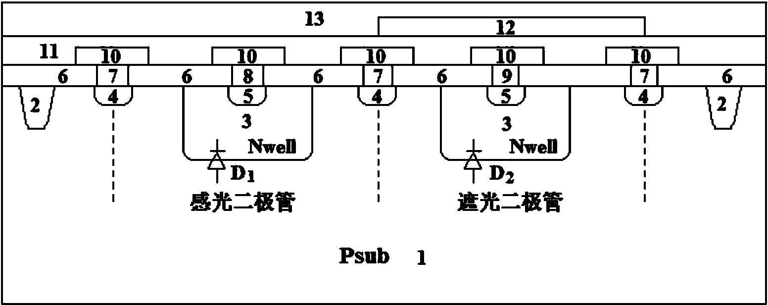
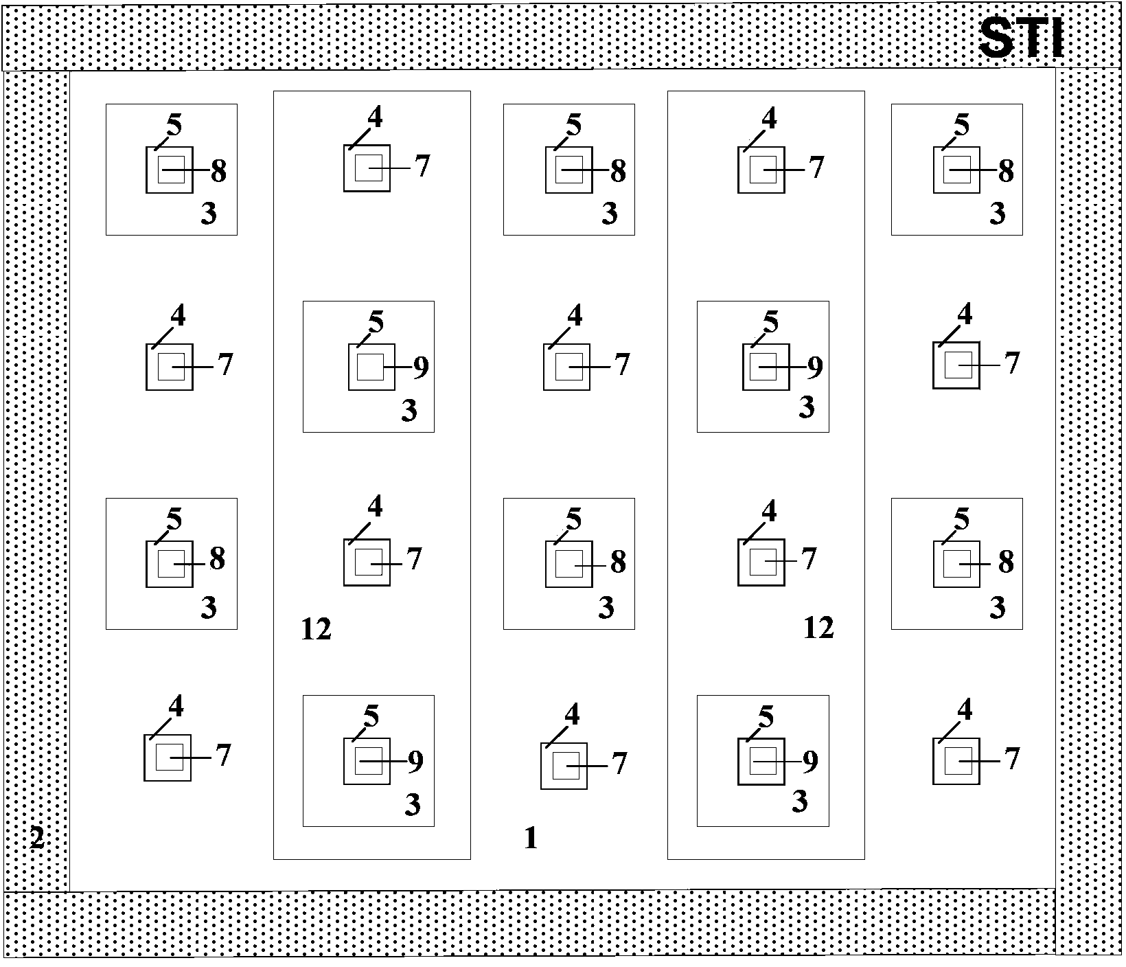
[0026] The invention belongs to the field of optical fiber communication system and optical interconnection, relates to a photodetector structure compatible with standard complementary metal oxide semiconductor (CMOS) technology, and involves the use of oxidation, photolithography, etching, ion implantation, metallization and other A series of standard CMOS process technologies realize the preparation method of this kind of detector, specifically, it relates to a photodetector with spatial modulation structure and its preparation method.

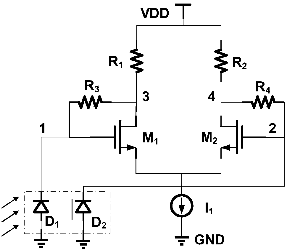
[0027] The present invention provides a photodetector for high-speed, high-responsiveness, and spatial modulation structure compatible with standard CMOS technology. The detector is composed of a photosensitive diode constructed by Nwell / Psub and a light-shielding diode constructed by the second-layer interconnection metal / Nwell / Psub. The spatial modulation of the input optical signal by the second-layer interconnection metal is used to elimi...


PUM


Abstract

The invention relates to an optical fiber communication system, optical interconnection and a photoelectric detector, and in order to provide the photoelectric detector which is high in PN-joint photodiode responsibility, wide in intrinsic bandwidth, and capable of achieving full differential output and to improve the overall performance of a standard CMOS technological monolithic integration photo receiver, the photoelectric detector of a spatial modulation structure is characterized in that a shallow groove separation area is manufactured on a P-type substrate, photodiodes and shading diodes are arrayed in the shallow groove separation area at intervals, the photodiodes are formed by N-type well regions with medium dosage concentration and the P-type substrate, the shading diodes are formed by N-type well regions with medium dosage concentration, the P-type substrate and a second interconnected metal layer, N-type well contact areas with heavy dosing are sequentially arranged on the N-type well regions with the medium dosage concentration, and P-type substrate contact areas with heavy dosing are arranged on the periphery of the N-type well regions with the medium dosage concentration. A preparation method of the photoelectric detector is mainly applied to design and manufacturing of photoelectric detectors.

Description

technical field [0001] The invention relates to an optical fiber communication system, an optical interconnection and a photodetector, in particular to a photodetector with a space modulation structure and a preparation method thereof. Background technique [0002] With the wide application of information and communication technology and the continuous emergence of various new services, user terminals have increasing requirements for network bandwidth. Traditional electrical interconnection networks are limited by RC delay, and it is difficult to further expand the frequency band. Therefore, using high-speed, high-capacity optical communication and optical interconnection to improve network performance has become an important research topic at present. As a key device in the field of optical communication and optical interconnection, the quality of photodetectors has a decisive impact on the performance of the entire system. [0003] At present, most of the receivers used i...

Claims


Application Information

Patent Timeline
Patent Type & Authority Applications(China)
IPC IPC(8): H01L27/14
Inventor 谢生刘娜毛陆虹张世林
Owner TIANJIN UNIV
Why Eureka
Try Eureka