Manufacturing method for N-shaped GaAs substrate laser diode

A technology of laser diode and manufacturing method, which is applied to lasers, laser parts, semiconductor lasers, etc., can solve the problems of crystal strain, degradation of the quality and performance of epitaxial layers on substrates, and shortened life of laser diodes, etc.

Inactive Publication Date: 2014-04-30
NANTONG MINICHIP MICRO ELECTRONICS
View PDF3 Cites 2 Cited by
  • Summary
  • Abstract
  • Description
  • Claims
  • Application Information

AI Technical Summary

Problems solved by technology

The above-mentioned semiconductor materials used as substrates generally contain various defects, such as dislocations, gaps or vacancies, etc. The defects will cause crystal strain, and the strain will reduce the quality and performance of the epitaxial layer on the substrate, resulting in a shortened life of the laser diode.

Method used


Image

  • Manufacturing method for N-shaped GaAs substrate laser diode

Examples


Embodiment Construction

[0016] The present invention will be described in detail below in conjunction with the accompanying drawings and specific embodiments, but not as a limitation of the present invention.

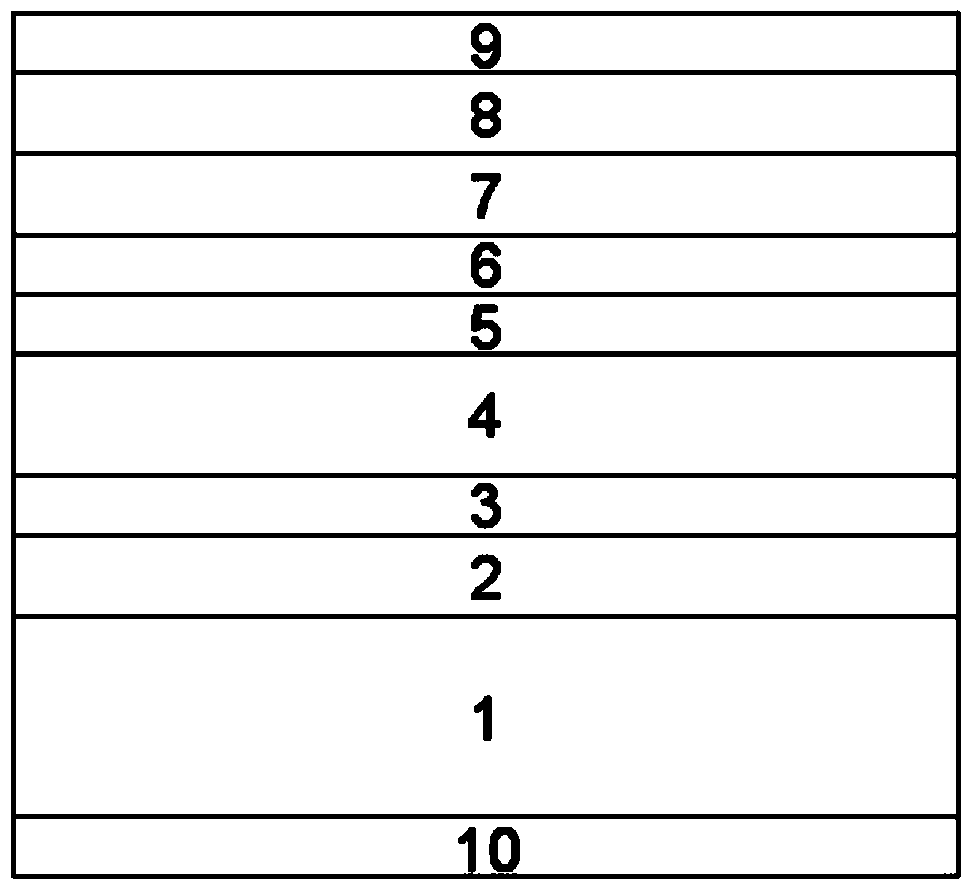
[0017] figure 1 A schematic diagram of the structure of the laser diode of the present invention is shown. It includes an n-GaAs substrate 1, on which an n-type cladding layer 2, an n-type light guide layer 3 and an active layer 4 are deposited in sequence.

[0018] The n-type cladding layer 2 is n-Al a In b Ga 1-a-b N, the optical guiding layer 3 is n-Al c In d Ga 1-c-d N, where 0≤a, b, c, d, a+b, c+d≤1.

[0019] The cladding layer 2 can also be n-Al a In b Ga 1-a-b N superlattice.

[0020] Active layer 4 is n-Al with superlattice structure e In f Ga 1-e-f N / n-AI g In h Ga 1-g-h N multiple quantum well layers, where 0≤e, f, g, h, e+f, g+h≤1.

[0021] A p-type barrier layer 5 is also deposited on the active layer 4, and the p-type barrier layer 5 is p-Al i In j Ga 1-i-j N,...


PUM


Abstract

The invention discloses a manufacturing method for an N-shaped GaAs substrate laser diode. The manufacturing method comprises the steps that a GaAs substrate is formed, and an n-shaped coating layer, an n-shaped light guide layer, an active layer, a p-shaped barrier layer, a p-shaped light guide layer and a p-shaped coating layer are sequentially deposited. The forming method of the GaAs substrate comprises the steps that a GaAs wafer is placed in a high-temperature high-pressure device, the GaAs wafer is heated and pressurized, the heating temperature ranges from 860 DEG C to 890 DEG C, pressure ranging from 5.0 GPa to 5.5 GPa is exerted, and the GaAs wafer is heated and pressurized for 10 minutes to 15 minutes; heating and pressing are stopped, and the GaAs wafer returns to a normal temperature and pressure state; annealing is conducted for 20 minutes-30 minutes in the high-temperature high-pressure device, and the GaAs wafer is taken out. According to the method, crystal defect density of the substrate of the laser diode can be obviously reduced, performance of the laser diode is enhanced, and service life of the laser diode is prolonged.

Description

technical field [0001] The invention relates to a manufacturing method of a laser diode. Background technique [0002] A laser diode (LD) is a diode formed of semiconductor materials, and its basic structure includes a substrate and a P / N cladding layer deposited on the substrate in sequence, an active layer and a P / N cladding layer, and a N Ohmic contacts on the P-type and P-type cladding layers. As the foundation of the building of LD, the substrate plays an important role. Sapphire is a commonly used LD substrate, but due to the lattice and thermal stress mismatch between it and the heterogeneous epitaxial layer on it, it will crack due to different expansion degrees after heating, resulting in device damage. Another type of LD substrate includes GaAs, GaAs, InP and other semiconductor materials. The above-mentioned semiconductor materials used as substrates generally contain various defects, such as dislocations, gaps or vacancies, etc. The defects will cause crystal ...

Claims


Application Information

Patent Timeline
IPC IPC(8): H01S5/343
Inventor 周明申云苏学杰段中明
Owner NANTONG MINICHIP MICRO ELECTRONICS
Why Eureka
Try Eureka