Single-layer-structure inverted top-emission OLED (Organic Light Emitting Device)

A single-layer structure, top emission technology, used in organic semiconductor devices, electrical solid devices, electrical components, etc., can solve the problems of electron and hole imbalance, unreported, etc., achieve low-efficiency roll-off, and expand the recombination area. , high efficiency

Inactive Publication Date: 2014-04-23
JILIN UNIV
View PDF4 Cites 8 Cited by
  • Summary
  • Abstract
  • Description
  • Claims
  • Application Information

AI Technical Summary

Problems solved by technology

Considering that the organic functional layer of a single-layer structure OLED can only transport a certain type of carrier, if a single-layer organic material with high electron mobility is introduced into the inverted top-emitting OLED as the matrix material, it can not only simplify the preparation of the device process, and through device structure design, the introduction of an organic dopant that captures holes can solve the problem of electron-hole imbalance in inverted top-emitting OLEDs. However, inverted top-emitting OLED devices with this structure are internationally recognized. Not yet reported

Method used


Image

  • Single-layer-structure inverted top-emission OLED (Organic Light Emitting Device)
  • Single-layer-structure inverted top-emission OLED (Organic Light Emitting Device)
  • Single-layer-structure inverted top-emission OLED (Organic Light Emitting Device)

Examples


Embodiment 1

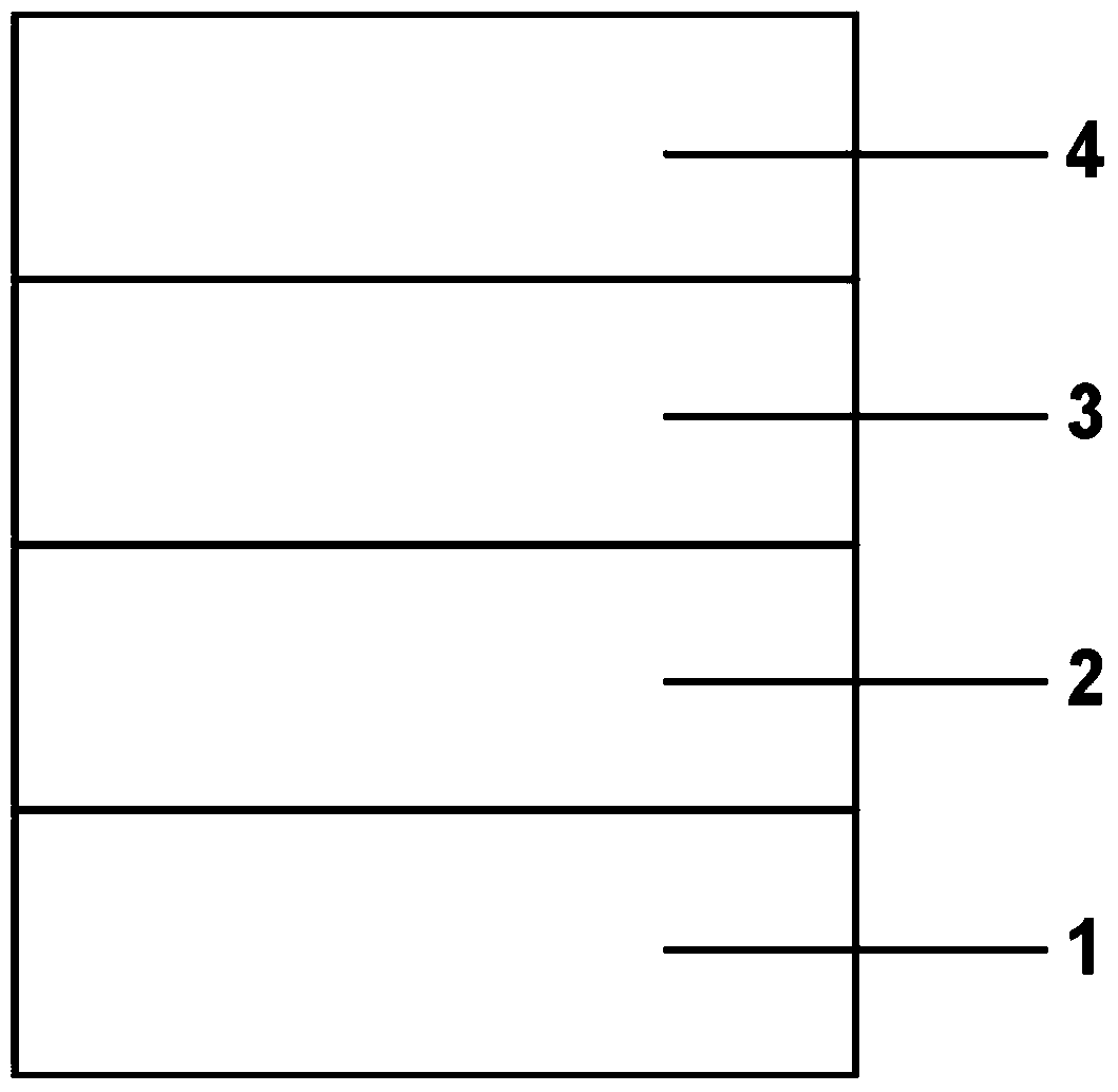
[0031] The structure of the prepared inverted top-emitting organic electroluminescent device is:

[0032] Device A: Si substrate / Mo(50nm) / Al(5nm) / Cs 2 CO 3 (1nm) / TPBi:10wt%FIrPic:6wt%PO-01(100nm) / MoO 3 (10nm) / Ag(20nm)

[0033] Device B: Si substrate / Mo(50nm) / Al(5nm) / Cs 2 CO 3 (1nm) / TPBi:6wt%PO-01(100nm) / MoO 3 (10nm) / Ag(20nm)

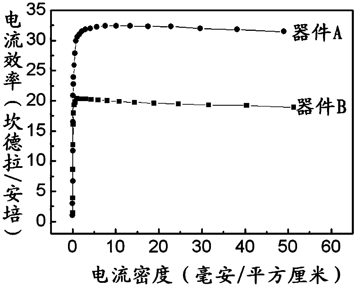
[0034] Wherein device A is a structure designed by the present invention, and device B is a comparative device doped with organic dye 1 only.

[0035] The preparation of the device can be carried out by a multi-source organometallic molecular vapor deposition system, and the detailed process is as follows:

[0036] [1] The substrate material in the experiment is a silicon substrate covered with a silicon dioxide insulating layer. First, the silicon substrate is repeatedly scrubbed with acetone and ethanol cotton balls;

[0037] [2] Put the scrubbed silicon substrate into a clean beaker and use acetone, ethanol, and deionized water to sonicate for...

Embodiment 2

[0041] The structure of the prepared inverted top-emitting organic electroluminescent device C is: silicon substrate / Mo(50nm) / Mg:Ag(5nm) / Cs 2 CO 3 (1nm) / TPBi:10wt%Ir(ppy) 3 :6wt%PO-01(100nm) / MoO 3 (10nm) / Ag(20nm). The volume ratio of Mg:Ag doping is 10:1, and the detailed process of device preparation is as in Example 1.

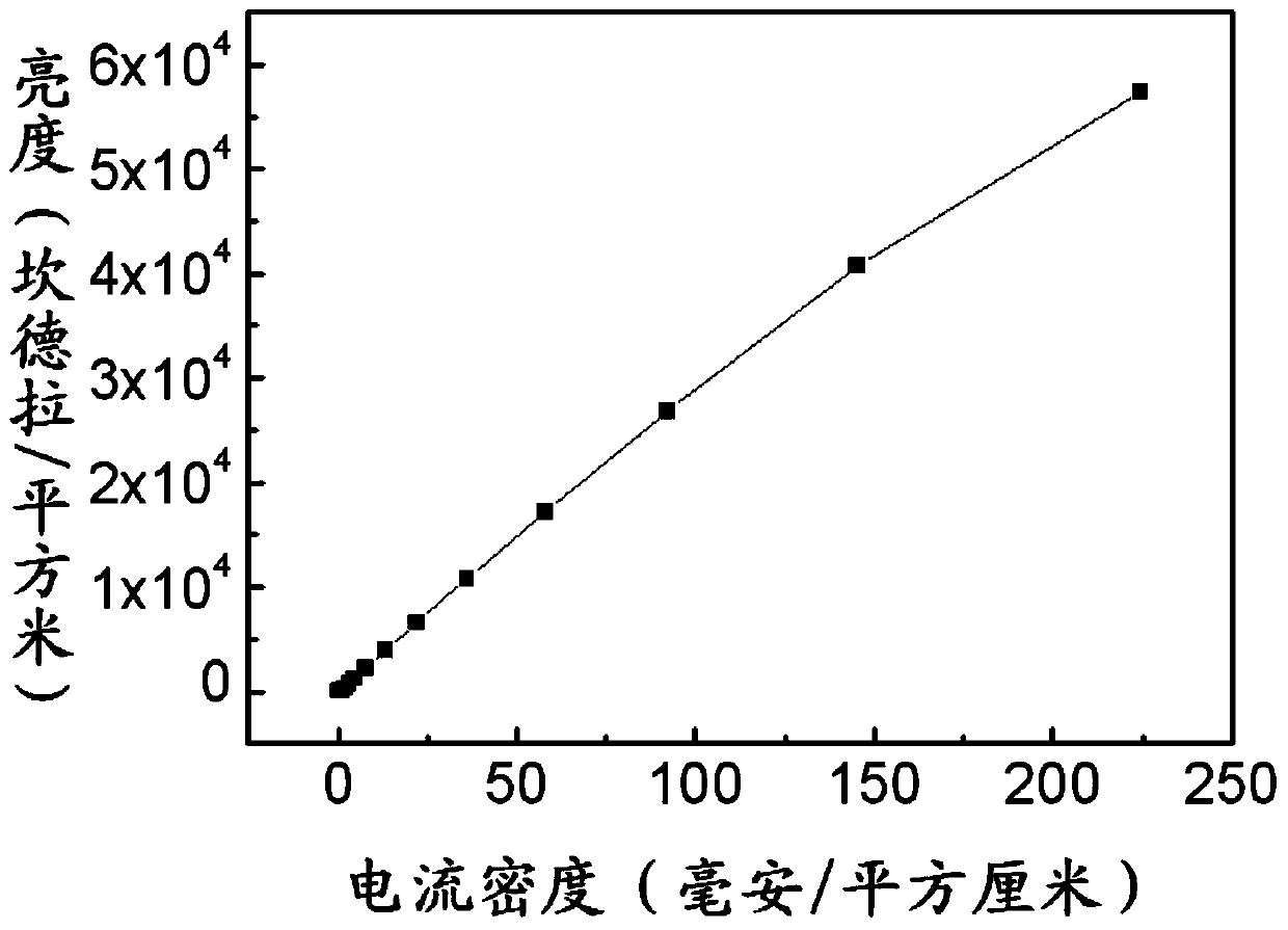
[0042] The brightness-current density of the inverted top-emitting device of the present invention is as follows image 3 shown. As can be seen from the figure, the maximum brightness of the device C designed by the present invention can reach 57384cd / m 2 . The maximum current efficiency of device C can reach 30.1cd / A. The current efficiency-brightness curve of device C is shown as Figure 4 As shown, device C is at 1000cd / m 2 The current efficiency at luminance is 26.3cd / A.


PUM


Abstract

The invention discloses a single-layer-structure inverted top-emission OLED (Organic Light Emitting Device), and belongs to the technical field of organic optoelectronic devices. The inverted top-emission OLED with the structure disclosed by the invention comprises a substrate, a cathode, a single-layer organic function layer and a transparent anode in sequence. The single-layer organic function layer is formed by doping two organic dyes into a single matrix material in a dopant mode, wherein the matrix material adopts an organic material with higher electron mobility, and the two organic dyes performs respective functions, namely, one organic dye is used for capturing holes, and the other organic dye is used for emitting light. According to the device with the structure disclosed by the invention, an exciton compound area is enlarged, the balance of electrons and holes in the single-layer organic function layer is favorably realized, and the device has the advantages of high efficiency, low efficiency roll-off, stability of light-emitting optical spectrum, and the like.

Description

technical field [0001] The invention belongs to the technical field of organic optoelectronic devices, and in particular relates to an inverted top-emitting organic electroluminescent device with a single-layer structure. Background technique [0002] Organic electroluminescent devices (OLEDs) have many advantages, such as solid-state luminescence, low energy consumption, active luminescence, wide viewing angle, fast response speed, easy realization of flexible display, and low cost. They have huge potential in the fields of color display and solid-state lighting. In terms of application value, many research institutions in the world have invested a lot of manpower and material resources to promote the rapid development of OLED technology. [0003] OLEDs can be divided into bottom-emitting OLEDs and top-emitting OLEDs according to how light is taken out. Bottom-emitting OLEDs have a contradiction between the display light-emitting area and the driving circuit of the pixel. ...

Claims


Application Information

Patent Timeline
Patent Type & Authority Applications(China)
IPC IPC(8): H01L51/52H01L51/50H01L51/54
CPCH10K71/16H10K85/111H10K50/121H10K50/805H10K2102/321
Inventor 陈平段羽薛凯文赵毅刘式墉
Owner JILIN UNIV
Why Eureka
Try Eureka