A High Voltage Super Junction Termination Structure

A junction terminal and terminal technology, applied in the field of high-voltage superjunction terminal structure, can solve the problems of increasing chip production cost, poor electric field uniformity, and increasing chip area, so as to reduce ion pollution and charge accumulation, and avoid electric field concentration effect. , the effect of preventing charge imbalance

Active Publication Date: 2016-08-17
INST OF MICROELECTRONICS CHINESE ACAD OF SCI
View PDF6 Cites 0 Cited by
  • Summary
  • Abstract
  • Description
  • Claims
  • Application Information

AI Technical Summary

Problems solved by technology

[0006] 1) It is difficult to ensure that the charges of the superjunction P and N columns are precisely balanced in the existing process, which will lead to the degradation of device parameters. For example, BV will drop sharply with the increase of charge imbalance.
[0007] 2) The uniformity of the electric field on the semiconductor surface of the terminal surface structure is not good, and it is easy to break down near the junction or at the end of the field plate
[0008] 3) The ion contamination and charge accumulation at the interface cannot be prevented in the process, which greatly affects the reliability of power devices
[0009] 4) Due to the pressure-resistant structure of the existing terminal technology, the width of the terminal surface structure domain required for high-voltage resistance is relatively large
Increases the chip area and increases the production cost of the chip

Method used


Image

  • A High Voltage Super Junction Termination Structure
  • A High Voltage Super Junction Termination Structure
  • A High Voltage Super Junction Termination Structure

Examples


Embodiment Construction

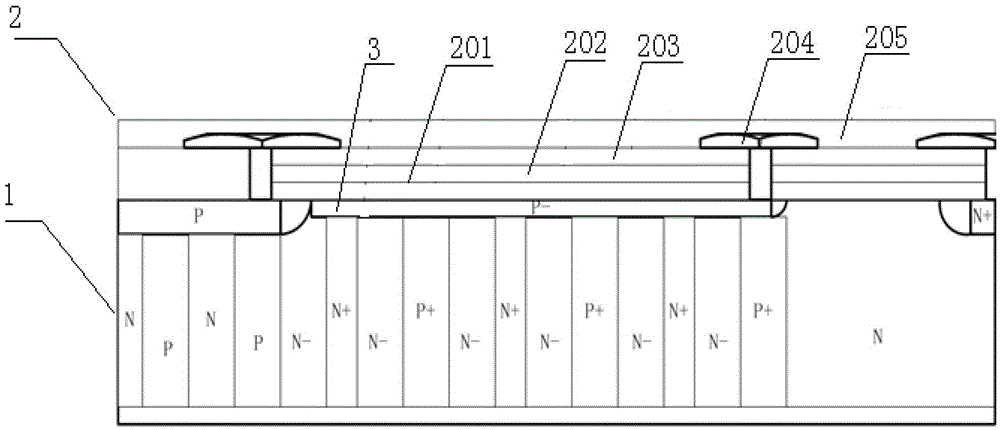
[0027] see figure 2 , the present invention provides a high-voltage super junction terminal structure, including a super junction region 1 composed of P+, N-, N+ columns distributed at intervals and a terminal surface structure 2 with a metal field plate and a SIPOS field plate, the super junction region 1 There is a layer of P-layer 3 between the terminal surface structure 2, and the surface of the terminal surface structure 2 silicon wafer is sequentially deposited with a high-resistance SIPOS layer 201, SiO 2 layer 202 , low-resistance SIPOS layer 203 , metal field plate 204 and nitrogen-doped SIPOS layer 205 .

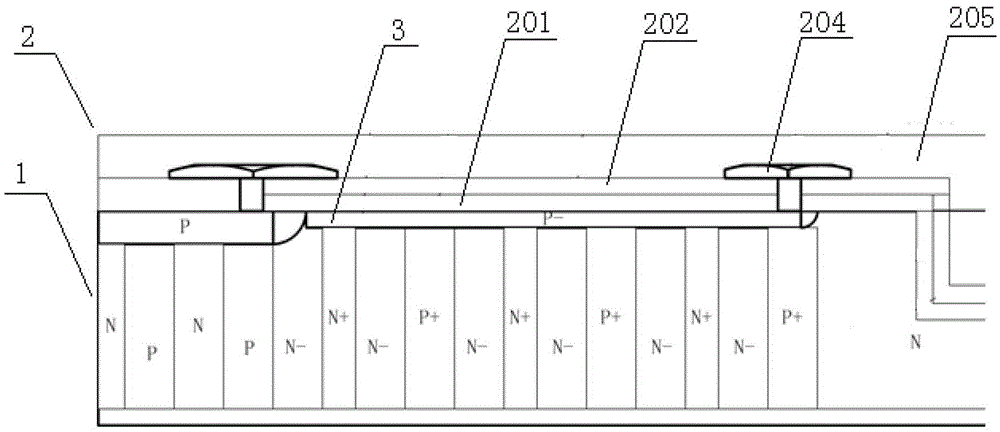
[0028] see image 3 , a high-voltage super-junction terminal structure provided by an embodiment of the present invention, including a super-junction region 1 composed of P+, N-, N+ columns distributed at intervals and a terminal surface structure 2 with a metal field plate and a SIPOS field plate, the super-junction There is a layer of P-layer 3 between the are...


PUM


Abstract

The invention provides a high-voltage super-junction terminal structure. The high-voltage super-junction terminal structure comprises a super-junction zone and a terminal surface structure, wherein the super-junction zone is formed through the spaced distribution of P+, N- and N+ poles; a metal field plate and an SIPOS (Semi-Insulating Polycrystalline Silicon) field plate are arranged on the terminal surface structure; a P- layer is arranged between the super-junction zone and the terminal surface structure; a high-resistance SIPOS layer, an SiO2 layer, a low-resistance SIPOS layer, the metal field plate and a nitrogen-doped SIPOS layer are sequentially deposited on the terminal surface structure from the bottom to the top, or the high-resistance SIPOS layer, the SiO2 layer, the metal field plate and the nitrogen-doped SIPOS layer are sequentially deposited on the terminal surface structure from the bottom to the top; the bottom end of the terminal surface structure is ended by a trench. The high-voltage super-junction terminal structure which is provided by the invention has the advantages that high voltage can be resisted, the reliability of the terminal is improved, and leaked current is reduced. The high-voltage super-junction terminal structure can be applied in the manufacture of the terminals of large power devices, such as an IGBT (Insulated Gate Bipolar Translator) and a VDMOS (Vertical Double Diffused Metal Oxide Semiconductor).

Description

technical field [0001] The invention relates to the field of manufacturing voltage-controlled power devices, in particular to a high-voltage super-junction terminal structure. Background technique [0002] The ability of a device to block high voltage mainly depends on the reverse bias breakdown voltage of a specific PN junction in the device structure. In power devices, due to the influence of PN junction bending or surface non-ideal factors at the termination of the PN junction, the reverse bias breakdown voltage of the PN junction is limited to occur near the surface or in the local area of ​​the junction bending relative to the parallel plane junction in the body. breakdown phenomenon. The junction terminal is a special structure specially designed to reduce the local electric field, improve the surface breakdown voltage and reliability, and make the actual breakdown voltage of the device closer to the ideal value of the parallel plane junction. In vertical conduction ...

Claims


Application Information

Patent Timeline
Patent Type & Authority Patents(China)
IPC IPC(8): H01L29/06H01L29/40
CPCH01L29/0634H01L29/0653
Inventor 王波朱阳军胡爱斌卢烁今
Owner INST OF MICROELECTRONICS CHINESE ACAD OF SCI
Why Eureka
Try Eureka