Forming method for multiple graphical mask layer and semiconductor structure
A multi-patterning and masking layer technology, which is applied in semiconductor devices, semiconductor/solid-state device manufacturing, electrical components, etc., can solve the problems of different shapes and affect the performance of semiconductor devices, and achieve the effect of reducing differences
- Summary
- Abstract
- Description
- Claims
- Application Information
AI Technical Summary
Problems solved by technology
Method used
Image

Examples
Embodiment Construction
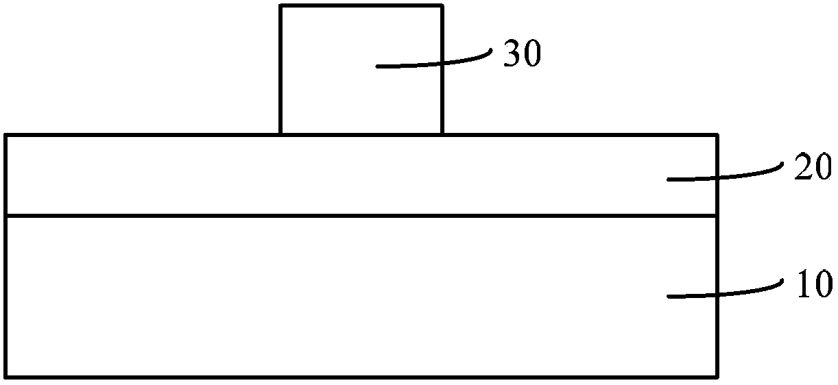
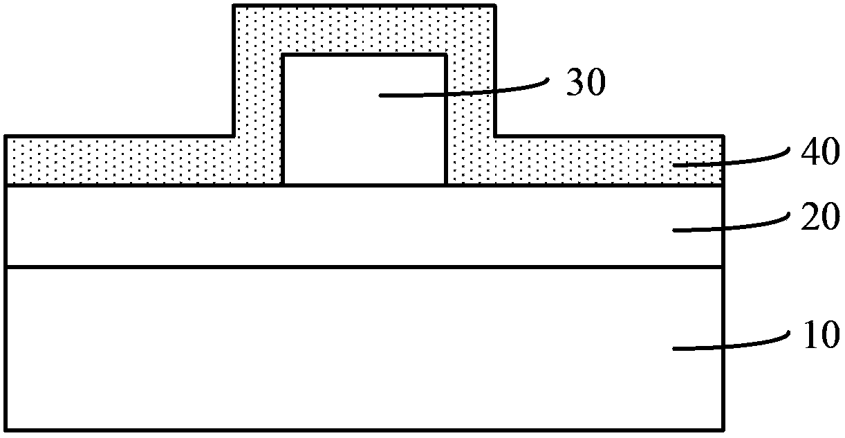
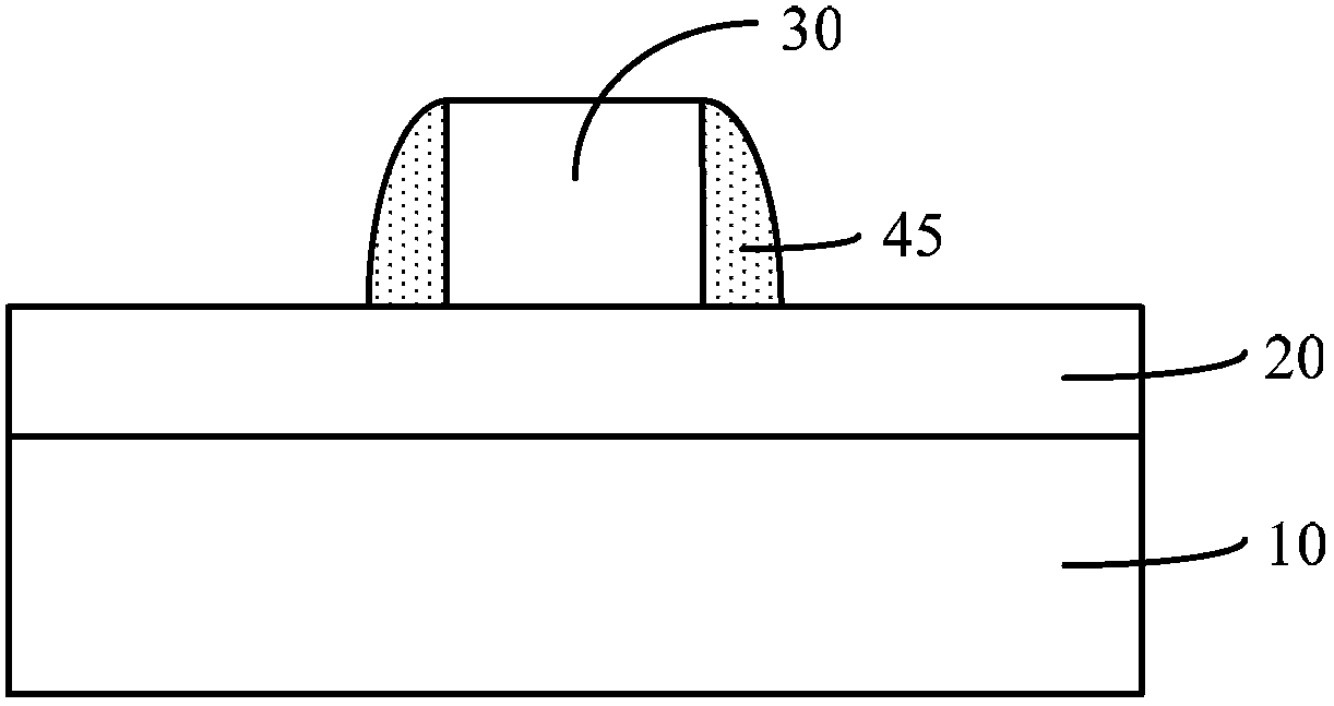
[0035] After the sidewalls formed by the self-aligned double patterning process in the prior art are used as masks to etch the material layer to be etched, the morphology of the sidewalls on both sides of the formed semiconductor pattern will be different, which will affect the quality of the subsequently formed semiconductor device. performance. The inventor found through research that in the existing self-aligned double patterning process, since the sidewall is formed by maskless etching of the hard mask material layer, the sidewall on the side of the sidewall in contact with the sacrificial layer is Vertical to the surface of the semiconductor substrate, the shape of the sidewall of the sidewall away from the side of the sacrificial layer is arc-shaped, and the closer to the top of the sidewall, the larger the arc, and the closer to the top of the sidewall, the shape of the sidewalls on both sides of the sidewall is arc-shaped. The greater the difference in appearance, the ...
PUM
| Property | Measurement | Unit |
|---|---|---|
| Thickness | aaaaa | aaaaa |
| Thickness | aaaaa | aaaaa |
Abstract
Description
Claims
Application Information
 - R&D
- Intellectual Property
- Life Sciences
- Materials
- Tech Scout
- Unparalleled Data Quality
- Higher Quality Content
- 60% Fewer Hallucinations
Browse by: Latest US Patents, China's latest patents, Technical Efficacy Thesaurus, Application Domain, Technology Topic, Popular Technical Reports.
© 2025 PatSnap. All rights reserved.Legal|Privacy policy|Modern Slavery Act Transparency Statement|Sitemap|About US| Contact US: help@patsnap.com