Liquid crystal display unit and device

A liquid crystal display device and liquid crystal display technology, applied in static indicators, nonlinear optics, instruments, etc., can solve the problems of over-dense arrangement, limitation of mechanism design, huge number of tape-and-reel chips, etc., to save space and reduce arrangement space. Effect

Inactive Publication Date: 2014-01-29
TCL CHINA STAR OPTOELECTRONICS TECH CO LTD
View PDF4 Cites 2 Cited by
  • Summary
  • Abstract
  • Description
  • Claims
  • Application Information

AI Technical Summary

Problems solved by technology

[0007] An object of the present invention is to provide a liquid crystal display device to solve the technical problem in the prior art that the mechanical design is limited due to the large number of tape chips arranged too densely along the lateral direction of the drive circuit board

Method used


Image

  • Liquid crystal display unit and device
  • Liquid crystal display unit and device
  • Liquid crystal display unit and device

Examples


Embodiment Construction

[0026] The following descriptions of the various embodiments refer to the accompanying drawings to illustrate specific embodiments in which the present invention can be practiced.

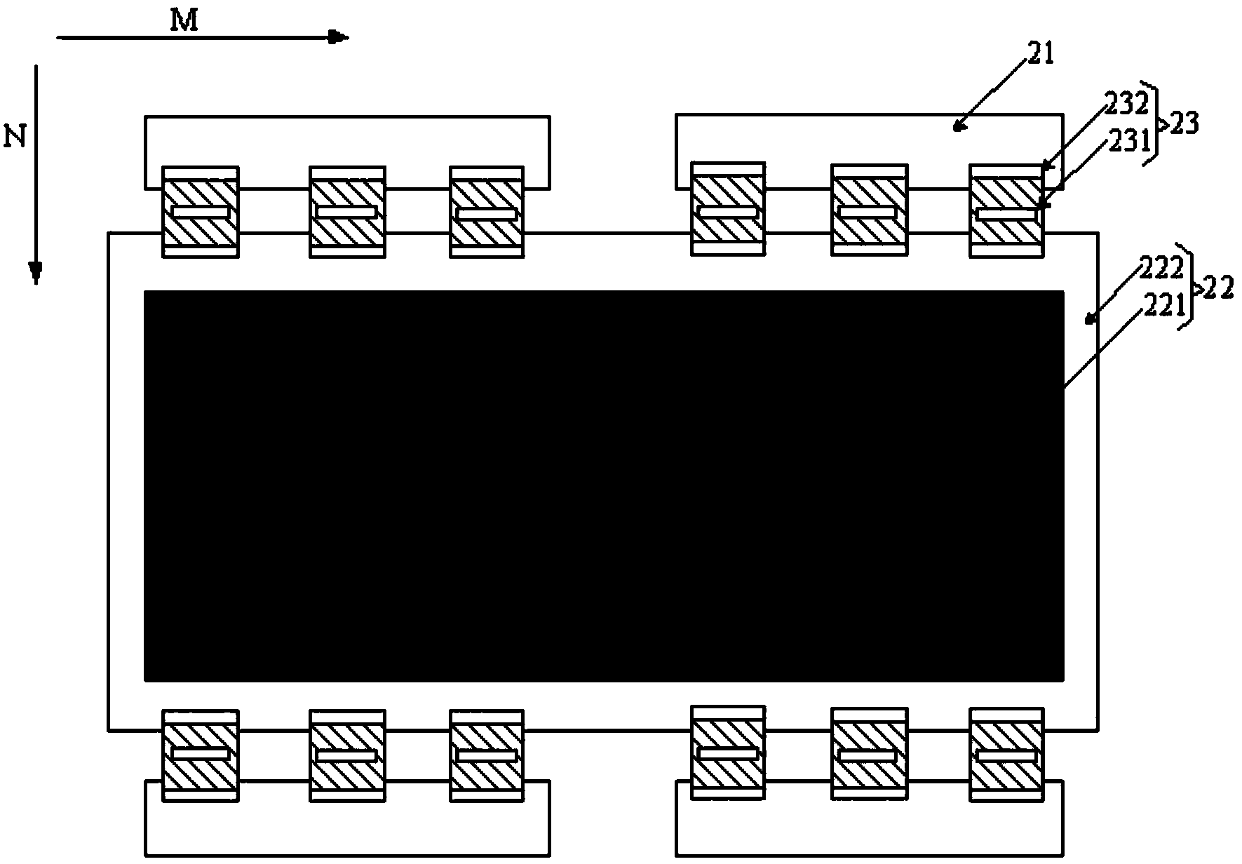
[0027] see figure 2 , figure 2 It is a schematic structural diagram of a liquid crystal display device provided by an embodiment of the present invention, which includes a driving circuit board 21 , a liquid crystal panel 22 and several connection units 23 .

[0028] The driving circuit board 21 extends along the transverse direction M, and the connecting units 23 are arranged along the transverse direction M, and each connecting unit 23 is respectively connected to the driving circuit board 21 and the liquid crystal panel 22 .

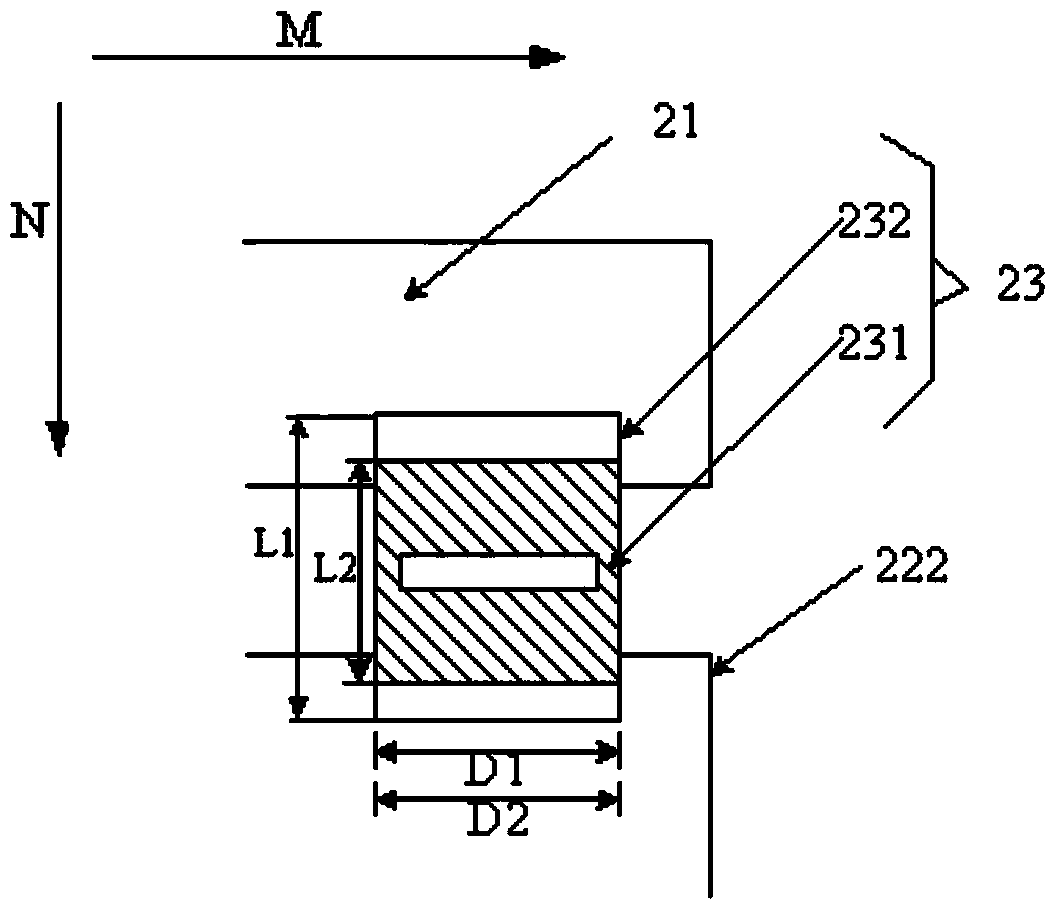
[0029] In the embodiment of the present invention, each connecting unit 23 includes at least two tape chips, such as two, three or more, and the at least two tape chips are covered (for example, please refer to Figure 5 ), and are connected to the driving circuit boar...


PUM


Abstract

The invention discloses a liquid crystal display unit and device. A plurality of connecting units are arranged between driving circuit boards and a liquid crystal display panel, every connecting unit comprises at least two tape coiling chips, and the at least two tape coiling chips are arranged in a covering mode and are all connected with the driving circuit boards and the liquid crystal display panel. Through the arrangement of the connecting units, the at least two tape coiling chips are formed on one of the connecting units in a concentrated mode, and accordingly the arrangement space in the extension direction of the driving circuit boards of the tape coiling chips can be reduced to save space, other designs such as the welding design of the tape coiling chips can be facilitated, or the addition of other devices and the like can be facilitated.

Description

【Technical field】 [0001] The invention relates to the technical field of liquid crystal display, in particular to a liquid crystal display device and equipment. 【Background technique】 [0002] With the continuous development of liquid crystal technology, the requirements for various components in the liquid crystal display device are getting higher and higher. [0003] Chip On Film (COF) packaging structures in the prior art basically use Tape Automated Bonding (TAB) technology for thermocompression packaging of the driver chip, and rolls For reel and feed. In use, each chip-on-flex structure can be sequentially cut from the tape substrate, and electrically connected between a transparent circuit on a glass substrate of a liquid crystal panel and a driving circuit board. There may be one or more flexible chip-on-chip structures between the glass substrate and the driving circuit board. The larger the size of the liquid crystal panel, the greater the number of flexible chip...

Claims


Application Information

Patent Timeline
IPC IPC(8): G02F1/13G02F1/133
CPCG02F1/13452
Inventor 李全
Owner TCL CHINA STAR OPTOELECTRONICS TECH CO LTD
Why Eureka
Try Eureka