
Fabrication method of multi-terminal quantum control devices based on bifurcated nanowires

A technology of nanowires and bifurcations, applied in the field of preparation of multi-terminal quantum control devices, to achieve the effect of uniform feature size, avoiding isolation process, and simple process

Active Publication Date: 2016-05-04
INST OF SEMICONDUCTORS - CHINESE ACAD OF SCI
View PDF3 Cites 0 Cited by
  • Summary
  • Abstract
  • Description
  • Claims
  • Application Information

AI Technical Summary

Problems solved by technology

[0005] On the other hand, research on Si-based interconnected optoelectronic devices has also entered a bottleneck

Method used


Image

  • Fabrication method of multi-terminal quantum control devices based on bifurcated nanowires
  • Fabrication method of multi-terminal quantum control devices based on bifurcated nanowires
  • Fabrication method of multi-terminal quantum control devices based on bifurcated nanowires

Examples


Embodiment Construction

[0025] It should be noted that, in the drawings or descriptions of the specification, similar or identical parts all use the same figure numbers. Implementations not shown or described in the accompanying drawings are forms known to those of ordinary skill in the art. Additionally, while illustrations of parameters including particular values ​​may be provided herein, it should be understood that the parameters need not be exactly equal to the corresponding values, but rather may approximate the corresponding values ​​within acceptable error margins or design constraints. In addition, the directional terms mentioned in the following embodiments, such as "upper", "lower", "front", "rear", "left", "right", etc., are only referring to the directions of the drawings. Accordingly, the directional terms are used to illustrate and not to limit the invention.

[0026] In an exemplary embodiment of the present invention, a method for preparing a bifurcated nanowire-based multi-termina...


PUM

PropertyMeasurementUnit
thicknessaaaaaaaaaa
lengthaaaaaaaaaa
thicknessaaaaaaaaaa

Abstract

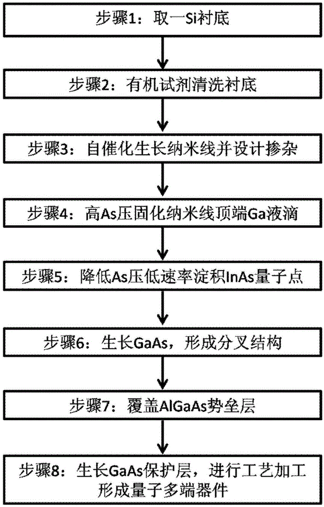
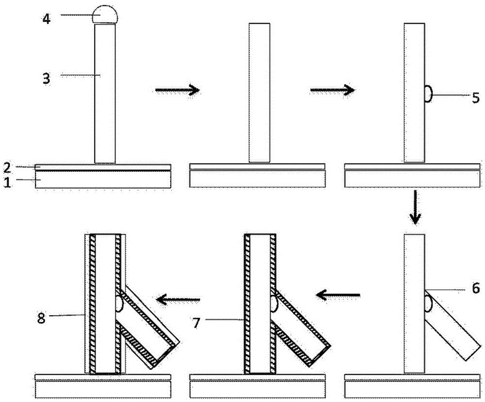
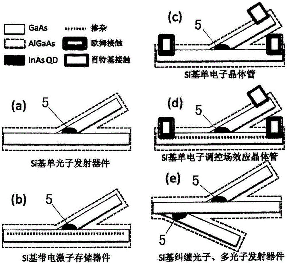
The invention discloses a preparation method of a multi-port quantum regulation and control device based on a bifurcated nanowire. The method comprises the following steps that 1, an Si substrate is taken; a naturally formed silica thin layer exists on the surface of the Si substrate; 2, the Si substrate is cleaned; 3, a GaAs nanowire is grown on the silica layer by an auto-catalysis method; N-type or P-type doping is selectively performed on the GaAs nanowire; 4, Ga drops at the top end of the GaAs nanowire are consumed by high As pressure treatment; growth of VLS (Vapor-Liquid-Solid) at the top end of the GaAs nanowire is restrained; 5, InAs quantum dots are deposited at a low speed on a side wall of the GaAs nanowire in a low As pressure environment; 6, a GaAs layer is grown on the InAs quantum dots; a bifurcated structure substrate is formed; 7, the bifurcated structure substrate is covered with an AlGaAs barrier layer; and 8, a GaAs protective layer is grown on the surface of the AlGaAs barrier layer; technology preparation is performed to form the multi-port quantum regulation and control device; and the preparation is accomplished.

Description

technical field [0001] The invention belongs to the technical field of semiconductor materials and devices, and relates to a preparation method of a bifurcated nanowire-based multi-terminal quantum control device. Background technique [0002] Semiconductor self-organized quantum dots are one of the most important solid-state quantum structures in the research of quantum physics and quantum information devices due to their "atom-like" properties. The emission, reading, manipulation, storage and parallel computing of high-quality single photons based on quantum dots are hot research directions. The controllable preparation of single quantum dots (such as precise positioning, ordered expansion, coupling with optical resonant cavity, etc.) and the realization of tunable optoelectronic devices are currently challenging issues. [0003] Quantum dots grown in the traditional S-K mode have the problem of positional randomness, which affects their effective coupling with the microc...

Claims


Application Information

Patent Timeline
Patent Type & Authority Patents(China)
IPC IPC(8): H01L21/02B82Y10/00
CPCH01L21/02463H01L21/02546H01L31/0304
Inventor 喻颖李密锋贺继方査国伟徐建星尚向军王莉娟倪海桥贺振宏牛智川
Owner INST OF SEMICONDUCTORS - CHINESE ACAD OF SCI
Learn More