


Quick Research
Generate reliable direction feasibility study reports for your R&D in just a few steps.

Technical Q&A
Discover and master advanced knowledge NOW. Basics, ideas, possibilities, all at once.

Find Solutions
As an expert in R&D theories, this can generate solutions to your technical problems instantly.

Evaluate Feasibility
Analyze your overall solution with one click, know your potential R&D risks in advance.

Monitor Landscape
Get weekly tech updates, stay abreast of the latest tech innovations and key insights.
Sintered compact and amorphous film
A technology of sintered body and amorphous film, applied in the directions of oxide conductors, non-metallic conductors, ion implantation plating, etc., can solve the problems of small refractive index, small specific resistance, and different composition systems
- Summary
- Abstract
- Description
- Claims
- Application Information
AI Technical Summary
Problems solved by technology
Method used
Image

Examples
Embodiment 1
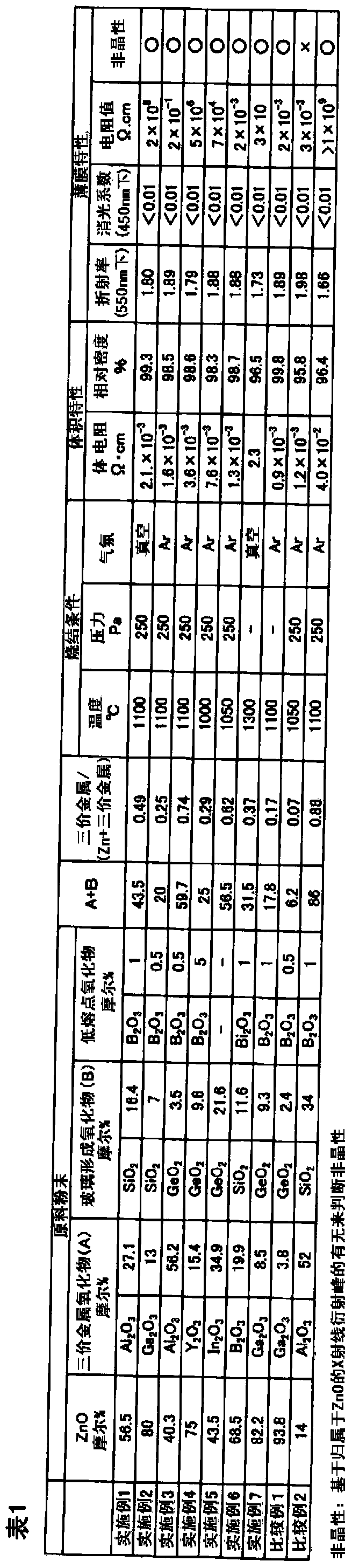
[0067] Prepare ZnO powder, Al 2 o 3 Powder, SiO 2 powder and B as a low-melting oxide 2 o 3 powder. Then, these powders were formulated into the proportions described in Table 1, and after they were mixed, the powder materials were placed in a vacuum at a temperature of 1100°C and a pressure of 250kgf / cm 2 Hot pressing sintering under the conditions.
[0068] Then, this sintered body was finished into a sputtering target shape by machining. The volume resistance and relative density of the obtained target were measured, and the results are shown in Table 1. The relative density reached 99.3%, the volume resistance was 2.1 mΩ·cm, and stable DC sputtering was possible.
[0069] In addition, sputtering was performed using the above-mentioned finished target. Set to DC sputtering, sputtering power 500W, containing 2 volume % O 2 Under the sputtering condition of the Ar gas pressure of 0.5Pa, the film is formed as film thickness. The amorphousness, refractive index (wavele...
Embodiment 2
[0072] Prepare ZnO powder, Ga 2 o 3 Powder, SiO 2 powder and B as a low-melting oxide 2 o 3 powder. Then, these powders were formulated into the proportions described in Table 1, and after they were mixed, the powder materials were heated in an argon atmosphere at a temperature of 1100° C. and a pressure of 250 kgf / cm 2 Hot pressing sintering under the conditions. Then, this sintered body was finished into a sputtering target shape by machining. The volume resistance and relative density of the obtained target were measured, and the results are shown in Table 1. The relative density reached 98.5%, the volume resistance was 1.6 mΩ·cm, and stable DC sputtering was possible.
[0073] In addition, sputtering was performed under the same conditions as in Example 1 using the above-mentioned finished target, and the amorphous property, refractive index (wavelength: 550 nm), volume resistivity, and extinction coefficient (wavelength: 450 nm) of the film-formed sample were measur...
Embodiment 3
[0075] Prepare ZnO powder, Al 2 o 3 Powder, GeO 2 powder and B as a low-melting oxide 2 o 3 powder. Then, these powders were formulated into the proportions described in Table 1, and after they were mixed, the powder materials were heated in an argon atmosphere at a temperature of 1100° C. and a pressure of 250 kgf / cm 2 Hot pressing sintering under the conditions. Then, this sintered body was finished into a sputtering target shape by machining. The volume resistance and relative density of the obtained target were measured, and the results are shown in Table 1. The relative density reached 98.6%, the volume resistance was 3.6 mΩ·cm, and stable DC sputtering was possible.
[0076] In addition, sputtering was performed under the same conditions as in Example 1 using the above-mentioned finished target, and the amorphous property, refractive index (wavelength: 550 nm), volume resistivity, and extinction coefficient (wavelength: 450 nm) of the film-formed sample were measur...
PUM
| Property | Measurement | Unit |
|---|---|---|
| electrical resistivity | aaaaa | aaaaa |
| electrical resistivity | aaaaa | aaaaa |
| electrical resistivity | aaaaa | aaaaa |
Abstract
Description
Claims
Application Information
 - R&D Engineer
- R&D Manager
- IP Professional
- Industry Leading Data Capabilities
- Powerful AI technology
- Patent DNA Extraction
Browse by: Latest US Patents, China's latest patents, Technical Efficacy Thesaurus, Application Domain, Technology Topic, Popular Technical Reports.
© 2024 PatSnap. All rights reserved.Legal|Privacy policy|Modern Slavery Act Transparency Statement|Sitemap|About US| Contact US: help@patsnap.com