
Texturing method of monocrystalline semiconductor substrates to reduce incident light reflectance

A single crystal semiconductor, texture technology, applied in semiconductor devices, semiconductor/solid-state device manufacturing, crystal growth and other directions, can solve problems such as reducing oxygen content

Inactive Publication Date: 2014-01-15
SUN CHEM CORP
View PDF4 Cites 0 Cited by
  • Summary
  • Abstract
  • Description
  • Claims
  • Application Information

AI Technical Summary

Problems solved by technology

To address this problem, a nitrogen purge is often used to reduce the oxygen content in the strong base bath; however, this purge does not reduce the oxygen content to low enough levels and planar regions are still typically observed

Method used


Image

  • Texturing method of monocrystalline semiconductor substrates to reduce incident light reflectance
  • Texturing method of monocrystalline semiconductor substrates to reduce incident light reflectance
  • Texturing method of monocrystalline semiconductor substrates to reduce incident light reflectance

Examples


Embodiment 1

[0059] Three doped monocrystalline silicon wafers (from SolarGiga) had n+ doped regions on the front or emitter layer and pn junctions below the emitter layer. The above-mentioned wafers were immersed in a large liquor ratio texturing solution in an 18 liter falcon line. The formulation of the texture solution is shown in Table 1.

[0060] Table 1

[0061] components

content

Tripropylene glycol 1

0.5wt%

Potassium hydroxide

6wt%

[0062] 1,4-Butanediol 2

0.5wt%

water

93wt%

[0063] 1 Weight average molecular weight=192g / mol; 2 Flash point = 121°C

[0064] Flash point=140.5℃

[0065] Boiling point=268℃

[0066] Each wafer was weighed prior to texturing. The aqueous texturing solution was 80°C. No nitrogen sparging. The solution was manually stirred. The pH of the texturing solution was 13. During the texturing process, the dissolved oxygen content was measured using a D0202G2-Wire Dissolve...

Embodiment 2

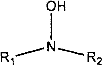
[0073] The method described in Example 1 was repeated using another three doped silicon single crystal semiconductor wafers. In addition to the components in Table 1, the formulation of the texturing solution included N-isopropylhydroxylamine. The formulation of the texture aqueous solution is shown in Table 3.

[0074] table 3

[0075] components

content

Tripropylene glycol

0.5wt%

Potassium hydroxide

6wt%

1,4-Butanediol

0.5wt%

N-isopropylhydroxylamine 3

0.017wt%

water

92.983wt%

[0076] 3 Hydroguard TM1-15 (Available from The Dow Chemical Company, Midland, MI, USA)

[0077] Each wafer was weighed before and after texturing. The aqueous texturing solution was 80°C. No nitrogen sparging. The solution was manually stirred. The pH of the texturing solution was 13. The results are shown in Table 4.

[0078] Table 4

[0079]

[0080] Addition of N-isopropylhydroxylamine reduces the oxygen c...

Embodiment 3

[0082] One of the two texturing solutions shown in Table 5 textured two doped monocrystalline silicon semiconductor wafers respectively.

[0083] table 5

[0084] components

Solution 1

Solution 2

Tripropylene glycol

1.2% bv

1.2% bv

Potassium hydroxide

6wt% (2ag / L)

6wt% (25g / L)

1,4-Butanediol

0.3% bv

0.3% bv

N-isopropylhydroxylamine

0.017wt%

water

margin

margin

[0085] Each wafer was immersed in one of the above two texturing solutions for 10 minutes. The solution was kept at 80°C and the pH of the solution was 13. Without nitrogen sparging, the solution was manually stirred. The oxygen content at the beginning of the texture in each bath was measured using a D0202G2-Wire Dissolved Oxygen Analyzer. Solution 1 containing no N-isopropylhydroxylamine had an oxygen content of 3.3 ppm. In contrast, solution 2 containing N-isopropylhydroxylamine had an oxygen content of 0 ppm. ...


PUM

PropertyMeasurementUnit
boiling pointaaaaaaaaaa
thicknessaaaaaaaaaa
thicknessaaaaaaaaaa

Abstract

The invention relates to a texturing method of monocrystalline semiconductor substrates to reduce incident light reflectance. Monocrystalline semiconductor substrates are textured with alkaline solutions to form pyramid structures on their surfaces to reduce incident light reflectance and improve light absorption of the wafers. The alkaline baths include compounds which inhibit the formation of flat areas between pyramid structures to improve the light adsorption. The method provided by the invention comprises a) providing a monocrystalline semiconductor substrate; b) providing a solution including one or more alkoxylated glycols comprising a molecular weight of 170 g / mole or greater and a flash point of 75 DEG C or greater, one or more alkaline compounds and one or more oxygen scavengers in sufficient amounts to reduce oxygen concentration in the solution to 1,000 ppb or less; and c)contacting the monocrystalline semiconductor substrate with the solution to anisotropically texture the monocrystalline semiconductor substrate.

Description

field of invention [0001] The invention relates to a texturing method of a single crystal semiconductor substrate which reduces the reflection of incident light. More specifically, the present invention relates to a texturing method of a single crystal semiconductor substrate in an alkaline bath, which reduces the reflection of incident light by reducing the plane area between pyramid structures. Background technique [0002] The textured semiconductor surface reduces the reflection of broadband incident light, thus increasing the intensity of absorbed light. These semiconductors can be used in the manufacture of solar cells. A solar cell is a device that converts incident light energy, such as sunlight, on its surface into electrical energy. Reducing the reflection of incident light on the surface can improve the power conversion efficiency. However, texturing is not limited to semiconductors for solar cells, but can also be used in photovoltaic devices, optical and elec...

Claims


Application Information

Patent Timeline
Patent Type & Authority Applications(China)
IPC IPC(8): H01L31/18H01L31/0236C30B33/10
CPCC30B33/10H01L31/02366H01L31/02168H01L31/02363Y02E10/50H01L21/306H01L31/042
Inventor R·K·巴尔C·奥康纳P·W·辛克利G·R·阿拉戴斯
Owner SUN CHEM CORP
Learn More