Bulk-silicon MOSFET structure
A variant, a technology of silicon metal, applied in the field of bulk silicon MOSFET structure, can solve the problems of high manufacturing cost, achieve low cost, suppress single-event radiation effect, and improve the effect of single-event radiation effect
- Summary
- Abstract
- Description
- Claims
- Application Information
AI Technical Summary
Problems solved by technology
Method used
Image
Examples
Embodiment Construction
[0016] The present invention is described in detail below in conjunction with accompanying drawing example:
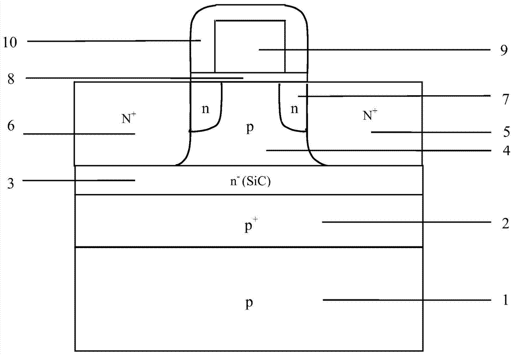
[0017] figure 1 Shown is the radiation-hardened structure of the bulk silicon MOSFET proposed in this paper. exist figure 1 Among them, 1 is p-type substrate; 2 is p + Low carrier lifetime silicon layer; 3 is n - SiC layer; 4 is p-type body region; 5 is N + Drain terminal; 6 is N + Source terminal; 7 is n-type LDD structure; 8 is gate oxide layer; 9 is polysilicon gate; 10 is Si 3 N 4 side wall.
[0018] Starting from the bottom of the device, above the p-type substrate 1 is a p + Low carrier lifetime silicon layer 2; p + An n - Layer 3 (also known as n - SiC layer or SiC layer), this layer is made of silicon carbide (SiC) material; above the SiC layer 3, the left and right sides are respectively the source region 6 of the device (also called N + source) and drain region 5 (also referred to as N + drain terminal), the middle is a p-type body region 4 , and...
PUM
| Property | Measurement | Unit |
|---|---|---|
| Doping concentration | aaaaa | aaaaa |
| Thickness | aaaaa | aaaaa |
| Thickness | aaaaa | aaaaa |
Abstract
Description
Claims
Application Information
 - R&D Engineer
- R&D Manager
- IP Professional
- Industry Leading Data Capabilities
- Powerful AI technology
- Patent DNA Extraction
Browse by: Latest US Patents, China's latest patents, Technical Efficacy Thesaurus, Application Domain, Technology Topic, Popular Technical Reports.
© 2024 PatSnap. All rights reserved.Legal|Privacy policy|Modern Slavery Act Transparency Statement|Sitemap|About US| Contact US: help@patsnap.com


