
Color image capturing element, image capturing device and image capturing program

A color imaging element and imaging element technology, applied in the field of color imaging elements, imaging devices, and imaging programs, can solve the problems of narrow opening of the light-shielding film, inability to excessively increase pixels for phase difference detection, and low sensitivity, so as to improve AF accuracy Effect

Inactive Publication Date: 2013-12-18
FUJIFILM CORP
View PDF11 Cites 4 Cited by
  • Summary
  • Abstract
  • Description
  • Claims
  • Application Information

AI Technical Summary

Problems solved by technology

[0015] In this AF operation, the more pixels for phase difference detection, the higher the accuracy. However, there is a problem that when an ordinary subject image is actually captured, the opening of the light-shielding film of the pixels for phase difference detection is narrow and the sensitivity is low. Cannot be processed in the same way as normal pixels, so the number of pixels for phase difference detection cannot be excessively increased

Method used


Image

  • Color image capturing element, image capturing device and image capturing program
  • Color image capturing element, image capturing device and image capturing program
  • Color image capturing element, image capturing device and image capturing program

Examples


no. 1 approach )

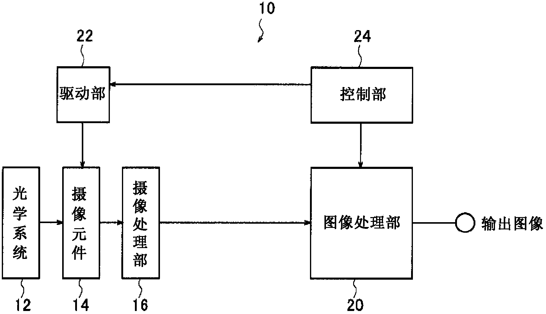
[0054] figure 1 A schematic block diagram of the imaging device 10 according to this embodiment is shown. The imaging device 10 is configured to include an optical system 12, an imaging element 14, an imaging processing unit 16, an image processing unit 20, a driving unit 22, and a control unit 24.

[0055] The optical system 12 is configured to include, for example, a lens group composed of a plurality of optical lenses, an aperture adjustment mechanism, a zoom mechanism, and an automatic focus adjustment mechanism.

[0056] The imaging element 14 is an imaging element including a plurality of photoelectric conversion elements arranged in the horizontal and vertical directions, such as CCD (Charge Coupled Device), CMOS (Complementary Metal Oxide Semiconductor), etc. A so-called single-plate image sensor with a structure where a color filter is arranged on the image sensor.

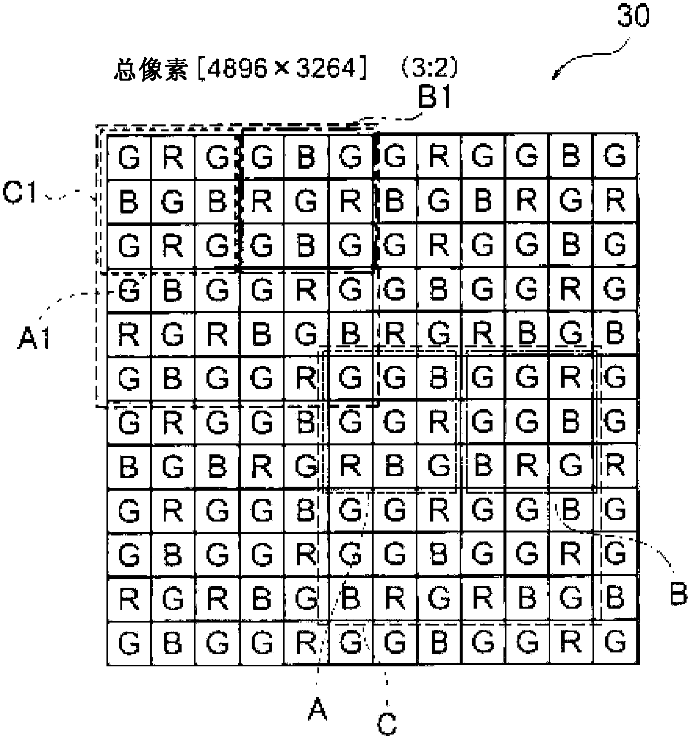
[0057] figure 2 A part of the color filter 30 according to this embodiment is shown. In addition, the numb...

no. 2 approach )

[0103] Next, the second embodiment of the present invention will be described. In addition, the same reference numerals are given to the same parts as in the first embodiment, and detailed descriptions thereof are omitted.

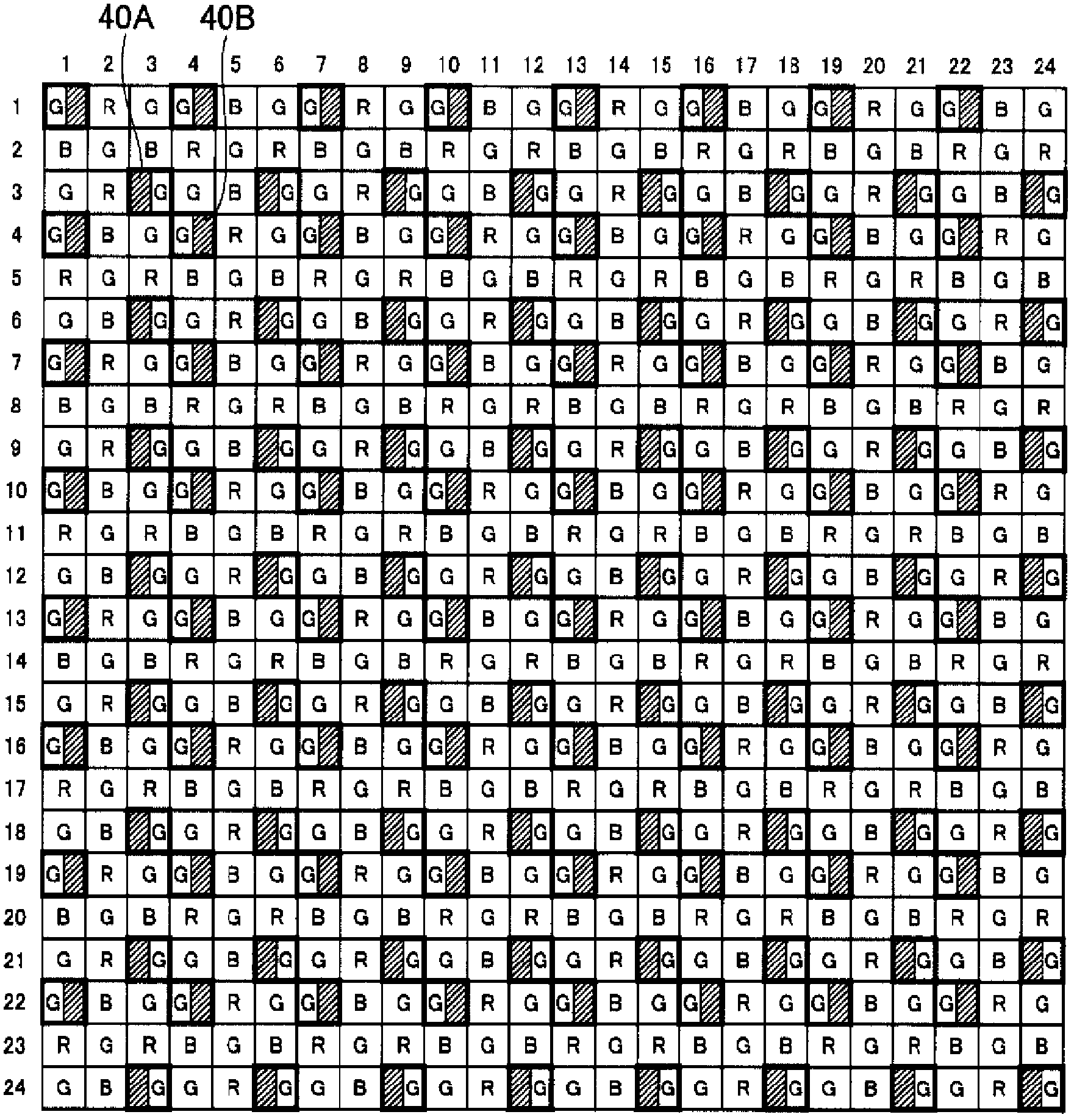
[0104] Image 6 The arrangement of the light-shielding films 40A and 40B according to this embodiment is shown. This embodiment is different from the first embodiment in the arrangement of light shielding films 40A and 40B.

[0105] Such as Image 6 As shown, in this embodiment, the light-shielding portion 40 is respectively provided on the upper first arrangement pattern A and the second arrangement pattern A and the second arrangement pattern B of the two first arrangement patterns A and the two second arrangement patterns B constituting the basic arrangement pattern C. On the phase difference detection pixels of the arrangement pattern B, all the basic arrangement patterns C are arranged. That is, in Image 6 In the example in the vertical direction, the l...

no. 3 approach )

[0109] Next, a third embodiment of the present invention will be described. In addition, the same reference numerals are given to the same parts as in the above-mentioned embodiment, and detailed descriptions thereof are omitted.

[0110] Figure 7 The arrangement of the light-shielding films 40A and 40B according to this embodiment is shown. This embodiment is different from the first embodiment in the arrangement of light shielding films 40A and 40B. The thinning drive is the same as in the second embodiment.

[0111] Such as Figure 7 As shown, in this embodiment, the light-shielding portion 40 is provided on the upper left 2× of the upper left first arrangement pattern A among the two first arrangement patterns A and the two second arrangement patterns B constituting the basic arrangement pattern C. On the two phase difference detection pixels on one of the two pixels diagonally, all the basic arrangement patterns C are arranged. That is, in Figure 7 In the example, the (6n...


PUM


Abstract

The purpose of the present invention is to improve the accuracy of phase difference AF control. An image capturing element (14) is provided with: a color filter (30) in which a basic arrangement pattern having a first arrangement pattern and a second arrangement pattern arranged to be symmetrical about a point is repeated, wherein the first arrangement pattern comprises first filters arranged on pixels in 2*2 arrangement located at the upper-left portion and a pixel located at the lower-right in a 3*3 pixel square arrangement, second filters arranged on the center and lower end lines in the vertical direction of the square arrangement, and third filters arranged on the center and right lines in the horizontal direction of the square arrangement, and wherein the second arrangement pattern comprises the first filters having the same arrangement as in the first arrangement pattern, and the second filters and the third filters having the arrangements interchanged with each other compared to the arrangements in the first arrangement pattern; and phase difference detection pixels arranged at positions corresponding to two pixels in the 2*2 pixel arrangement of at least one first arrangement pattern or second arrangement pattern, among all first arrangement patterns and the second arrangement patterns constituting the basic arrangement pattern.

Description

Technical field [0001] The present invention relates to a color imaging element, an imaging device, and an imaging program, and more particularly to a color imaging element, an imaging device, and an imaging program including pixels for phase difference detection. Background technique [0002] In order to improve the AF (autofocus) performance of solid-state imaging devices mounted in imaging devices such as digital cameras, there is a technology that uses some of the pixels formed on the light-receiving surface of the solid-state imaging device as phase difference detection pixels ( For example, refer to Patent Documents 1 to 7). [0003] The phase difference detection pixels are, for example, as described in Patent Documents 1 to 7 below. They are composed of a pair of adjacent two pixels equipped with filters of the same color, and are provided with smaller apertures than the light-shielding film provided in ordinary pixels. The shading film opening. Furthermore, the light-shi...

Claims


Application Information

Patent Timeline
Patent Type & Authority Applications(China)
IPC IPC(8): H04N9/07H04N5/232
CPCH04N23/672H04N25/445H04N25/704H04N25/134
Inventor 青木贵嗣林健吉远藤宏河村典子井上和纪
Owner FUJIFILM CORP
Learn More