led packaging method

A technology of LED packaging and LED chips, which is applied in the direction of electrical components, electric solid devices, circuits, etc., can solve the problems of uneven light color of the light source and easy formation of light spots, and achieve no light spots, high light efficiency and reliability, and light color uniform effect

Active Publication Date: 2015-10-21
FUJIAN TIANDIAN OPTOELECTRONICS CO LTD
View PDF4 Cites 0 Cited by
  • Summary
  • Abstract
  • Description
  • Claims
  • Application Information

AI Technical Summary

Problems solved by technology

[0003] Most of the existing LED packaging adopts dispensing or pressure injection to form lenses, so that the light color of the packaged light source is not uniform, and it is easy to form light spots

Method used


Image

  • led packaging method
  • led packaging method
  • led packaging method

Examples


Embodiment Construction

[0022] It should be noted that, in the case of no conflict, the embodiments in the present application and the features in the embodiments can be combined with each other. The present invention will be further described in detail below in conjunction with the drawings and specific embodiments.

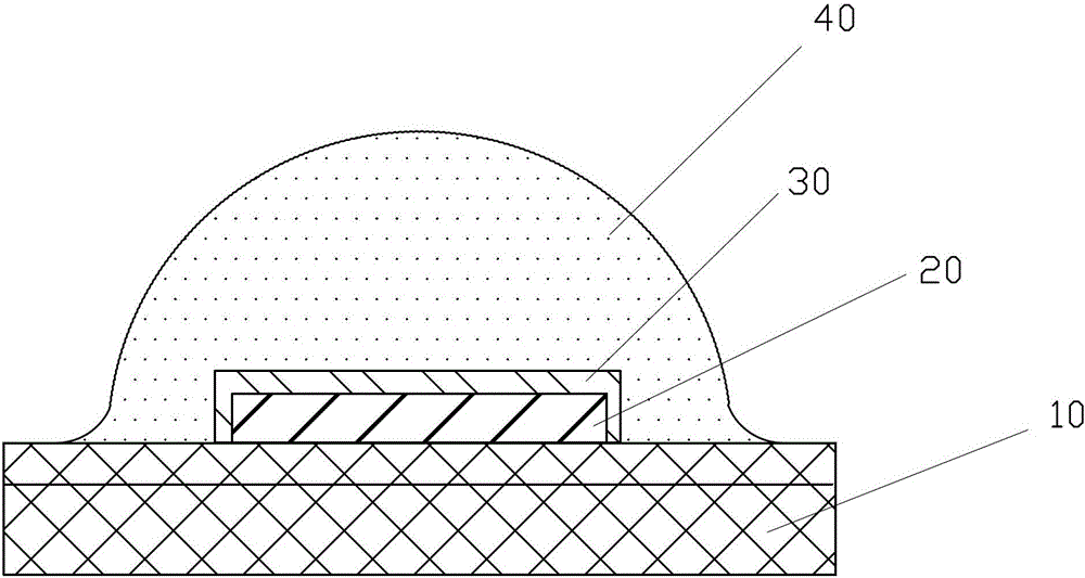
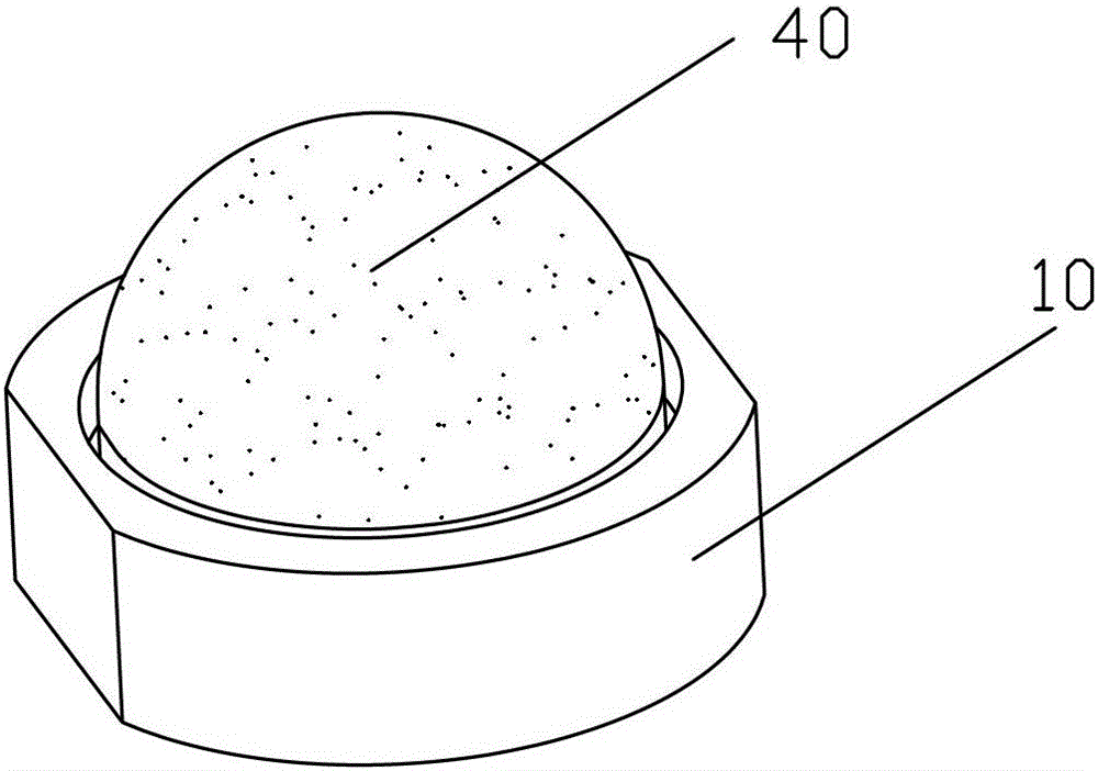
[0023] Please refer to figure 1 , is a schematic cross-sectional view of a specific embodiment of the LED packaging structure of the present invention. The LED packaging structure provided in this embodiment includes: a substrate 10 , an LED chip 20 , a fluorescent glue layer 30 and an optical structure layer 40 .

[0024] The substrate 10 can be a metal frame, ceramic or metal substrate. The substrate 10 is preferably a ceramic substrate 10 with high thermal conductivity. By virtue of the high thermal conductivity ceramic substrate, the heat dissipation of the LED packaging structure is good,

[0025] The quality is stable and reliable.

[0026] The LED chips 20 are fixed on the s...


PUM


Abstract

An embodiment of the invention relates to an LED encapsulation structure and an encapsulation method. The LED encapsulation structure comprises a substrate, an LED chip fixed to the substrate, a fluorescent glue layer formed on the outside of the LED chip and an optical structure layer formed on the outer side of the fluorescent glue layer in a pressing injection mode, wherein the surface of the optical structure layer undergoes atomization processing. The surface of the optical structure layer undergoing the atomizing processing by means of an atomization film is uneven, so that diffuse reflection of an LED light source is generated. Therefore, light colors are uniform, light spots caused by uneven light colors are avoided, and luminous efficacy and reliability are high.

Description

technical field [0001] The invention relates to LED packaging technology, in particular to an LED packaging structure and packaging method. Background technique [0002] Light Emitting Diode (LED) is a solid-state semiconductor device that can convert electrical energy into light. It is widely used in display screens, traffic signals, display light sources, automotive lights, LED backlights, and lighting sources. . [0003] Most of the existing LED packaging adopts dispensing or pressure injection to form lenses, so that the light color of the packaged light source is not uniform, and it is easy to form light spots. Contents of the invention [0004] The technical problem to be solved by the embodiments of the present invention is to provide an LED packaging structure and packaging method to achieve uniform light color of the light source, no light spots, and high light efficiency and reliability. [0005] In order to solve the above technical problems, the embodiment of...

Claims


Application Information

Patent Timeline
Patent Type & Authority Patents(China)
IPC IPC(8): H01L33/48H01L33/58H01L25/075
Inventor 陈栋周印华万喜红雷玉厚方春玲
Owner FUJIAN TIANDIAN OPTOELECTRONICS CO LTD
Why Eureka
Try Eureka