Infrared semiconductor laser active region, semiconductor laser and manufacturing method thereof

A manufacturing method and semiconductor technology, applied in the direction of semiconductor lasers, lasers, laser components, etc., can solve the problems that III-V semiconductor materials cannot be used in the wavelength range, and laser diodes have not been successfully developed, so as to reduce the interfacial recombination rate, Effects of improving performance and life, and reducing optical loss

Active Publication Date: 2015-12-23
SUZHOU INST OF NANO TECH & NANO BIONICS CHINESE ACEDEMY OF SCI
View PDF4 Cites 0 Cited by
  • Summary
  • Abstract
  • Description
  • Claims
  • Application Information

AI Technical Summary

Problems solved by technology

In addition, the current traditional III-V semiconductor materials that are lattice-matched with binary crystals cannot be applied to the wavelength range greater than 4 μm
II-VI compound semiconductors have semiconductor materials that can emit wavelengths greater than 2 μm. HgCdTe has been widely studied and applied as an infrared detector material. However, only the stimulated emission of 3.8-4.1 μm and 3- Spontaneous emission at 15 μm, no reports of successfully developed laser diodes

Method used


Image

  • Infrared semiconductor laser active region, semiconductor laser and manufacturing method thereof
  • Infrared semiconductor laser active region, semiconductor laser and manufacturing method thereof
  • Infrared semiconductor laser active region, semiconductor laser and manufacturing method thereof

Examples


Embodiment 1

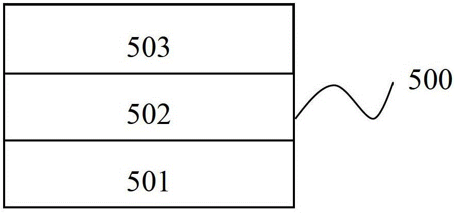
[0036] This embodiment takes a single quantum well laser with a wavelength of 4 μm as an application example to further illustrate the technical solution of the present invention, but this should not limit the protection scope of the present invention.

[0037] like figure 1 As shown, the active region 500 of the infrared semiconductor laser is a single quantum well structure, and the material of the potential well layer 502 is In m Ga 1-m As 1-n Bi n , wherein the composition m of In is 0.008, and the composition n of Bi is 0.028; the material of barrier layers 501, 503 is In x Ga 1-x As 1-y Bi y , where the values ​​of the components x and y of In and Bi gradually change from 0.48 to 0.54 and 0.04 to 0 respectively in the direction away from the potential well layer.

[0038] In this embodiment, a waveguide layer (attached figure 1 Not shown in ), the material of the waveguide layer is In x Ga 1-x As 1-y P y ; The waveguide layer is a graded waveguide layer, and ...


PUM


Abstract

The invention discloses an active area of an infrared semiconductor laser. The active area comprises a quantum well structure, wherein a potential well layer in the quantum well structure is made from InmGa1-mAs1-nBin; a potential barrier layer in the quantum well structure is made from InxGa1-xAs1-yBiy, m is equal to 0.48 to 0, n is equal to 0.04 to 0.34, x is equal to 0.48 to 0.54 and y is equal to 0.04 to 0. As InxGa1-xAs1-yBiy is adopted as the material of the active area of the semiconductor laser, based on lattice matching growth, the active area can be compatible with DBR, DFB, vertical-cavity surface-emitting lasers and other laser structures, and the laser adopting the Al-free structure improves the device performance and prolongs the device service life. The invention further provides a semiconductor laser and a manufacturing method thereof.

Description

technical field [0001] The invention relates to the field of semiconductor optoelectronics, in particular to an active region of an infrared semiconductor laser, a semiconductor laser including the active region and a manufacturing method thereof. Background technique [0002] Semiconductor lasers with a radiation wavelength greater than 2 μm are collectively referred to as mid- and far-infrared semiconductor lasers. They have growing prospects in high-resolution gas molecular spectrometers and are useful tools for measuring trace components in the air. In addition, in the mid-infrared band of 3-5 μm, the minimum loss of non-oxide waveguides, such as thallium bromide and chalcogenide stripping, can reach 10 -2 ~10 -5 dB / km, indicating that it is possible to open up a new field of extremely low-loss optical communication. Obviously, this type of laser must be a direct transition semiconductor with a narrow band. [0003] Although many quaternary system materials in the III...

Claims


Application Information

Patent Timeline
Patent Type & Authority Patents(China)
IPC IPC(8): H01S5/343
Inventor 赵勇明董建荣李奎龙孙玉润曾徐路于淑珍赵春雨杨辉
Owner SUZHOU INST OF NANO TECH & NANO BIONICS CHINESE ACEDEMY OF SCI
Why Eureka
Try Eureka