An integrated thin film solar cell module and its preparation method
A solar cell and integrated technology, applied in the field of solar photovoltaic power generation, can solve the problems of reduced photoelectric conversion efficiency, complex series process of integrated solar energy, and poor reliability, and achieve the effect of fewer electrical connection points, high reliability, and simple process
- Summary
- Abstract
- Description
- Claims
- Application Information
AI Technical Summary
Problems solved by technology
Method used
Image
Examples
Embodiment 1
[0067] This embodiment provides a method for connecting thin-film solar cell units in an integrated thin-film solar cell module in series, which includes the following steps:
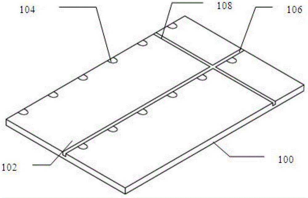
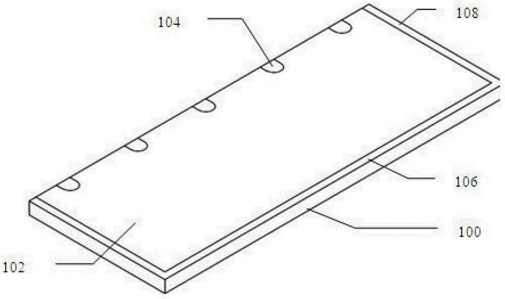
[0068] Step 1: Prepare several independent thin-film solar cell units, such as figure 2 As shown, the thin-film solar cell unit includes a flexible conductive substrate 100 and a photovoltaic layer 102 disposed on the flexible substrate 100, and the same side of the thin-film solar cell unit is provided with several recesses toward the inside of the photovoltaic layer 102. interconnection region 104, to expose a partial region of the flexible conductive substrate 100;
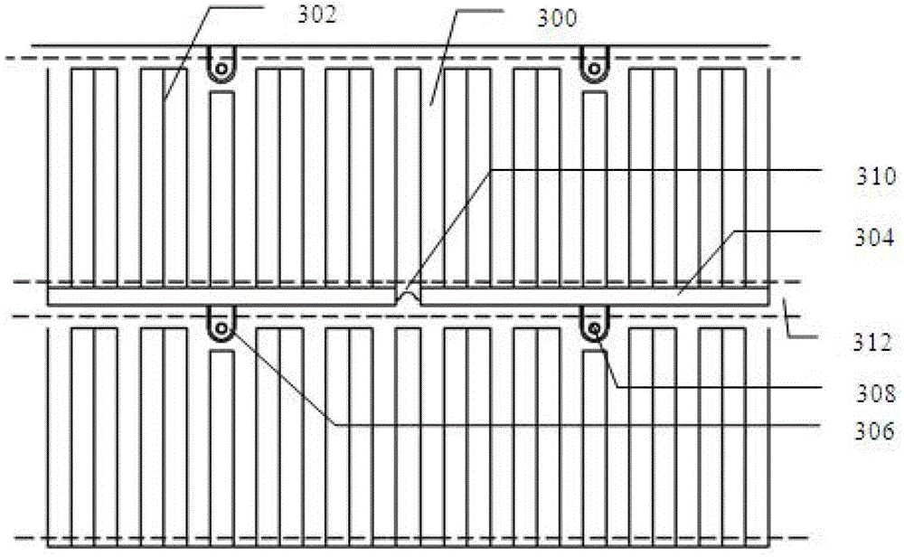
[0069] Step 2: Prepare several conductive patterns 300 that are independent of each other and arranged in an array. The conductive pattern 300 includes a bus 304, a gate line 302 connected to the same side of the bus 304, and a gate line 302 extending from the other side of the bus 304. Interconnection strips 306, the position interval...
Embodiment 2
[0074] This embodiment provides an integrated thin-film solar cell assembly and a manufacturing method thereof. The integrated thin-film solar cell assembly includes a solar cell assembly, a diode assembly and a rear sheet 500 sequentially arranged on a front sheet 400 .
[0075] The solar module includes a number of thin-film solar cell units divided by thin-film solar cells, and the adjacent thin-film solar cell units are connected in series; the front plate 400 is also provided with a number of conductive patterns that are independent of each other and arranged in an array 300, an insulating strip 312 is provided at the interval adjacent to the conductive pattern 300, the width of the insulating strip 312 is greater than the interval width of the adjacent conductive pattern 300, and the thin film solar cell unit is arranged on the conductive pattern 300 above; the diode assembly includes several thin film diodes 502 arranged on the back of the thin film solar cell unit, and ...
PUM
 Abstract
Description
Claims
Application Information
 - R&D Engineer
- R&D Manager
- IP Professional
- Industry Leading Data Capabilities
- Powerful AI technology
- Patent DNA Extraction
Browse by: Latest US Patents, China's latest patents, Technical Efficacy Thesaurus, Application Domain, Technology Topic, Popular Technical Reports.
© 2024 PatSnap. All rights reserved.Legal|Privacy policy|Modern Slavery Act Transparency Statement|Sitemap|About US| Contact US: help@patsnap.com


