


Quick Research
Generate reliable direction feasibility study reports for your R&D in just a few steps.

Technical Q&A
Discover and master advanced knowledge NOW. Basics, ideas, possibilities, all at once.

Find Solutions
As an expert in R&D theories, this can generate solutions to your technical problems instantly.

Evaluate Feasibility
Analyze your overall solution with one click, know your potential R&D risks in advance.

Monitor Landscape
Get weekly tech updates, stay abreast of the latest tech innovations and key insights.
Method for increasing surface area of inductor
A technology of surface area and inductance, applied in the field of increasing the surface area of inductance, can solve the problems of large winding distance and low density, and achieve the effect of improving performance, large winding density and increasing effective surface area
- Summary
- Abstract
- Description
- Claims
- Application Information
AI Technical Summary
Problems solved by technology
Method used
Image

Examples
Embodiment Construction
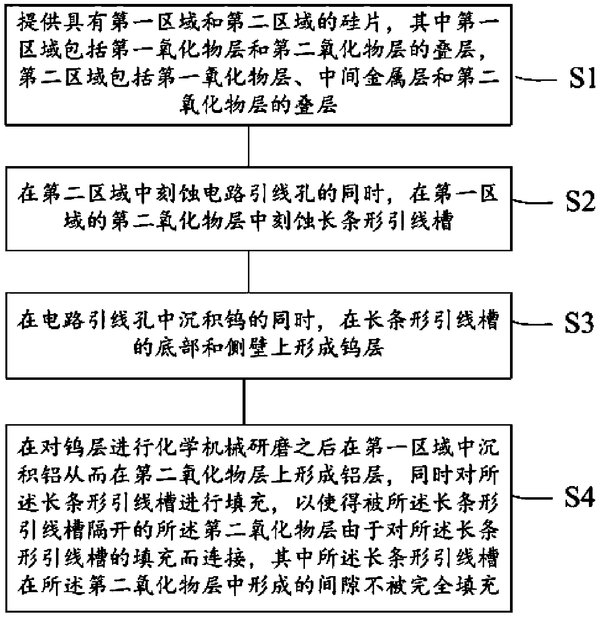
[0021] In order to make the content of the present invention clearer and easier to understand, the content of the present invention will be described in detail below in conjunction with specific embodiments and accompanying drawings.
[0022] figure 1 A flow chart of a method for increasing the surface area of an inductor according to an embodiment of the present invention is schematically shown.
[0023] Specifically, as figure 1 As shown, the method for increasing the surface area of an inductor according to an embodiment of the present invention includes:
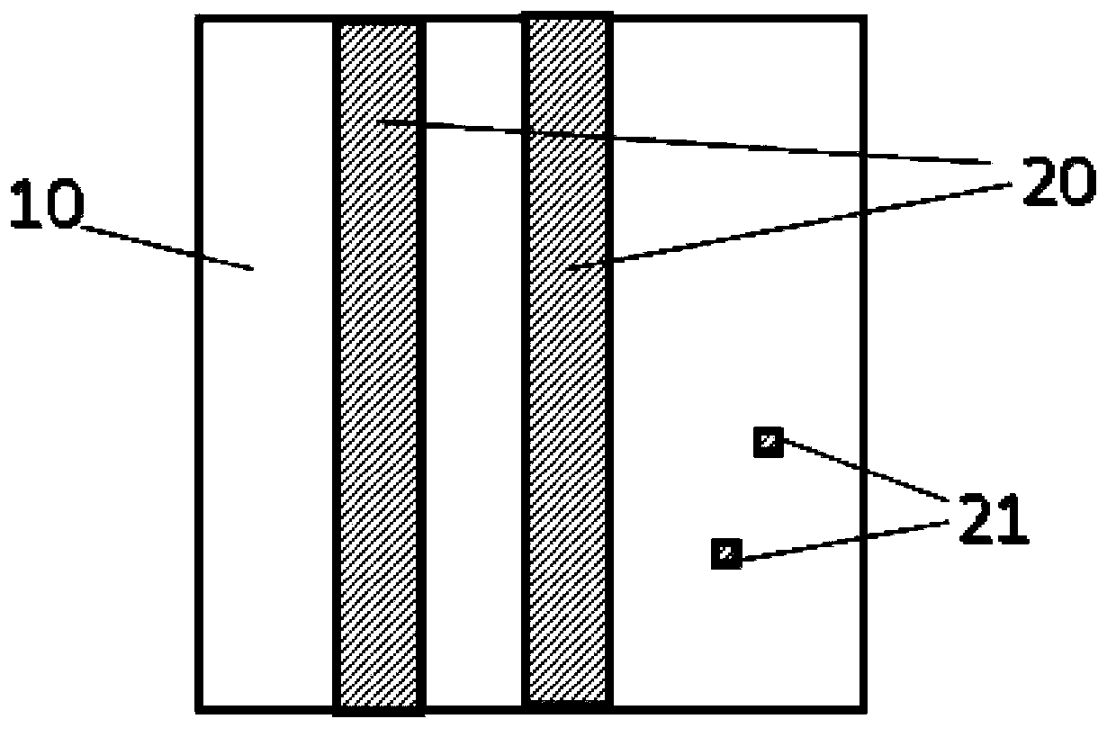
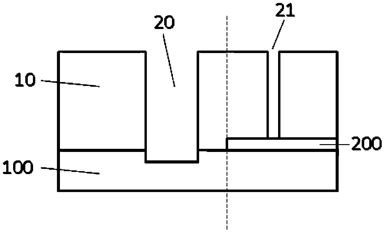
[0024] First step S1: providing a silicon wafer having a first region and a second region, wherein the first region includes a stack of the first oxide layer 100 and the second oxide layer 10, and the second region includes the first oxide layer 100 , the stack of the intermediate metal layer 200 and the second oxide layer 10, such as image 3 As shown in the cross-sectional diagram of , the left side of the dotte...
PUM
 Abstract
Description
Claims
Application Information
 - R&D Engineer
- R&D Manager
- IP Professional
- Industry Leading Data Capabilities
- Powerful AI technology
- Patent DNA Extraction
Browse by: Latest US Patents, China's latest patents, Technical Efficacy Thesaurus, Application Domain, Technology Topic, Popular Technical Reports.
© 2024 PatSnap. All rights reserved.Legal|Privacy policy|Modern Slavery Act Transparency Statement|Sitemap|About US| Contact US: help@patsnap.com