Infrared multi-wavelength absorber
A multi-wavelength, absorber technology, used in the field of infrared electromagnetic wave absorption and detection, can solve the problems of large thickness of the resonant absorber, insensitive to structural polarization, and difficult to control absorption characteristics, and achieves simple structure, improved sensitivity, and easy absorption characteristics. control effect
- Summary
- Abstract
- Description
- Claims
- Application Information
AI Technical Summary
Problems solved by technology
Method used
Image

Examples
Embodiment 1
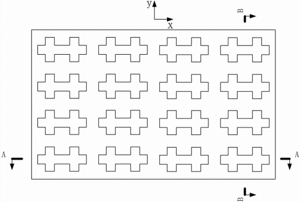
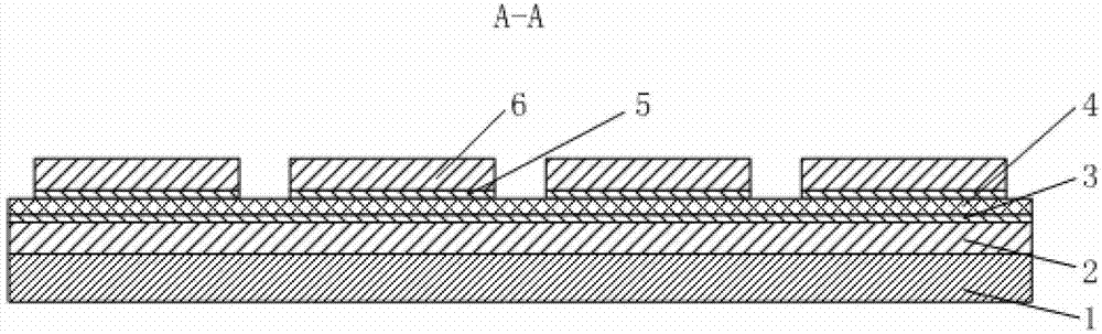
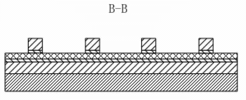
[0021] See attached figure 1 , Attached figure 2 , Attached image 3 The infrared dual-wavelength absorber proposed by the present invention includes a substrate I1, a structural layer I2, an adhesive layer I3, a dielectric layer 4, an adhesive layer II5, and a structural layer II6. The material of the substrate I1 is Si, the structural layer I2 and the structure The material of layer Ⅱ6 is Au, the material of adhesion layer Ⅰ3 and adhesion layer Ⅱ5 are both Ti, and the material of dielectric layer 4 is Al 2 O 3 The length of the double cross structure in the x direction is 1.2 μm, the length in the y direction is 0.8 μm, the width of the double cross arm is 0.3 μm, the period in the x direction is 2 μm, and the period in the y direction is 1.2 μm; the thickness of the structural layer Ⅰ 2 and the structural layer Ⅱ 6 are both It is 0.1 μm, the thickness of the dielectric layer 4 is 0.05 μm, and the thickness of the adhesion layer I3 and the adhesion layer II5 is 5 nm. See atta...
Embodiment 2
[0023] See attached figure 1 , Attached figure 2 , Attached image 3 The infrared dual-wavelength absorber proposed by the present invention includes a substrate I1, a structural layer I2, an adhesive layer I3, a dielectric layer 4, an adhesive layer II5, and a structural layer II6. The material of the substrate I1 is Si, the structural layer I2 and the structure The material of layer Ⅱ6 is Au, the material of adhesion layer Ⅰ3 and adhesion layer Ⅱ5 are both Ti, and the material of dielectric layer 4 is Al 2 O 3 The length of the double cross structure in the x direction is 1.4μm, the length in the y direction is 0.8μm, the width of the double cross arm is 0.3μm, the period in the x direction is 2μm, and the period in the y direction is 1.2μm; the thickness of the structural layer I2 and the structural layer II6 are both It is 0.1 μm, the thickness of the dielectric layer 4 is 0.05 μm, and the thickness of the adhesion layer I3 and the adhesion layer II5 is 5 nm. See attached ...
Embodiment 3
[0025] See attached figure 1 , Attached figure 2 , Attached image 3 The infrared dual-wavelength absorber proposed by the present invention includes a substrate I1, a structural layer I2, an adhesive layer I3, a dielectric layer 4, an adhesive layer II5, and a structural layer II6. The material of the substrate I1 is Si, the structural layer I2 and the structure The material of layer Ⅱ6 is Au, the material of adhesion layer Ⅰ3 and adhesion layer Ⅱ5 are both Ti, and the material of dielectric layer 4 is Al 2 O 3 The length of the double cross structure in the x direction is 1.6μm, the length in the y direction is 0.8μm, the width of the double cross arm is 0.3μm, the period in the x direction is 2μm, and the period in the y direction is 1.2μm; the thickness of the structural layer I2 and the structural layer II6 are both It is 0.1 μm, the thickness of the dielectric layer 4 is 0.05 μm, and the thickness of the adhesion layer I3 and the adhesion layer II5 is 5 nm. See attached ...
PUM
| Property | Measurement | Unit |
|---|---|---|
| thickness | aaaaa | aaaaa |
| thickness | aaaaa | aaaaa |
| thickness | aaaaa | aaaaa |
Abstract
Description
Claims
Application Information
 - R&D
- Intellectual Property
- Life Sciences
- Materials
- Tech Scout
- Unparalleled Data Quality
- Higher Quality Content
- 60% Fewer Hallucinations
Browse by: Latest US Patents, China's latest patents, Technical Efficacy Thesaurus, Application Domain, Technology Topic, Popular Technical Reports.
© 2025 PatSnap. All rights reserved.Legal|Privacy policy|Modern Slavery Act Transparency Statement|Sitemap|About US| Contact US: help@patsnap.com