Electrode of full-back-contact solar cell and fabrication method of electrode
A solar cell and full back contact technology, applied in the field of solar cells, can solve problems such as current collection and easy grid breakage, and achieve the effects of reducing influence, reducing line resistance loss, and improving performance
- Summary
- Abstract
- Description
- Claims
- Application Information
AI Technical Summary
Problems solved by technology
Method used
Image
Examples
Embodiment
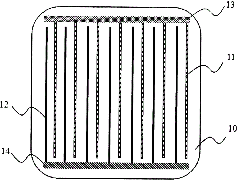
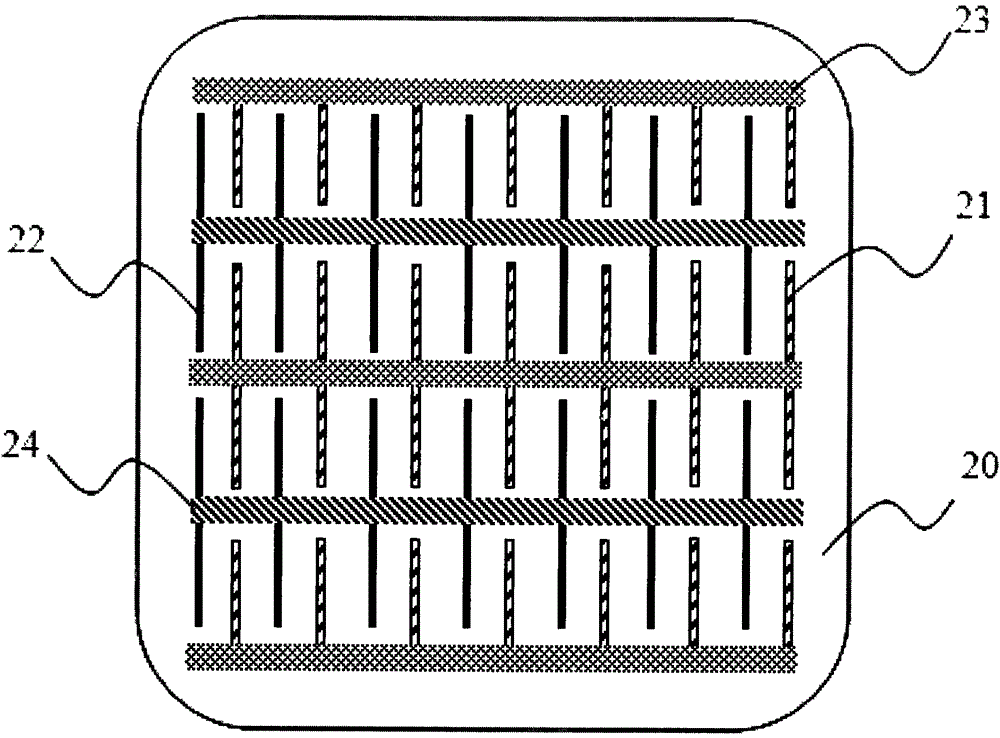
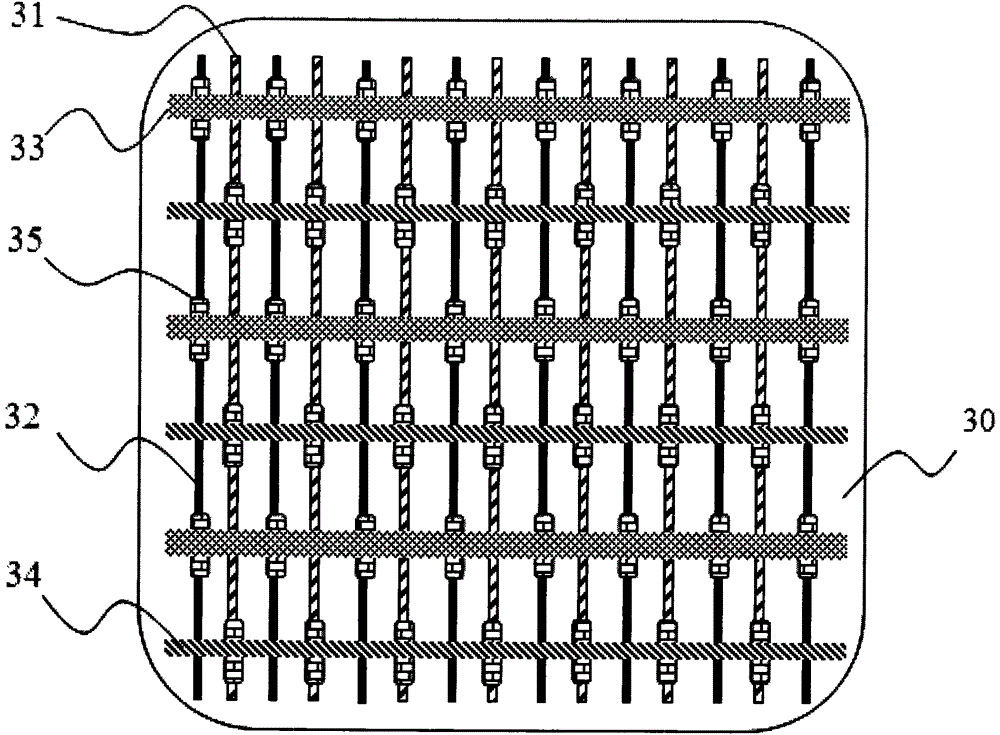
[0038] Embodiment: The embodiment of the present invention discloses a full back contact solar cell electrode, the electrode structure of which is as follows Figure 3-5 Shown:
[0039] Prepare interdigitated alternately arranged p-type doped regions 37 and n-type doped regions 38 on the back of an n-type single crystal silicon substrate with a resistivity of 0.5-20.0 ohm·cm, for example 1.0 ohm·cm;
[0040] Dielectric layer 2 36 is deposited on p-type doped region 37 and n-type doped region 38, and the composition of dielectric layer 2 36 can be silicon nitride, silicon oxide, silicon oxynitride, as silicon nitride, and its thickness is in Between 30 and 300 nanometers, such as 80 nanometers;
[0041] Fine grid metal electrode 1 31, fine grid metal electrode 2 32, main grid electrode 1 33, and main grid electrode 2 34 are deposited on the dielectric layer 2 36; fine grid metal electrode 1 31 and fine grid metal electrode 2 32 form a fork The fingers are arranged alternately...
PUM
| Property | Measurement | Unit |
|---|---|---|
| thickness | aaaaa | aaaaa |
| width | aaaaa | aaaaa |
Abstract
Description
Claims
Application Information
 - Generate Ideas
- Intellectual Property
- Life Sciences
- Materials
- Tech Scout
- Unparalleled Data Quality
- Higher Quality Content
- 60% Fewer Hallucinations
Browse by: Latest US Patents, China's latest patents, Technical Efficacy Thesaurus, Application Domain, Technology Topic, Popular Technical Reports.
© 2025 PatSnap. All rights reserved.Legal|Privacy policy|Modern Slavery Act Transparency Statement|Sitemap|About US| Contact US: help@patsnap.com


