A kind of polymer solar cell and preparation method thereof
A solar cell and polymer technology, applied in circuits, photovoltaic power generation, electrical components, etc., can solve the problems of affecting the photoelectric conversion efficiency of batteries, affecting the electrical properties such as the resistance of solar cell devices, open-circuit voltage fill factor, and low photoelectric conversion efficiency. , to achieve the effect that the fill factor is not reduced, the photoelectric conversion efficiency is improved, and the open circuit voltage is not reduced.
- Summary
- Abstract
- Description
- Claims
- Application Information
AI Technical Summary
Problems solved by technology
Method used
Image
Examples
Embodiment 1
[0039] The first step is to prepare a transparent anode: ultrasonically clean the G / ITO with electrode pattern etched with concentrated hydrochloric acid for 10 minutes in deionized water, absolute ethanol, acetone, and isopropanol, blow dry with nitrogen, and treat with UV / ozone 20min.
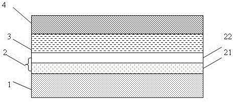
[0040] In the second step, the first hole transport layer is prepared on the transparent anode, and the Ag nanoparticles with a particle size of 50nm are doped in the PEDOT:PSS aqueous solution to prepare a 5.0% mixed solution by weight, which is coated by spin coating , and then dried at 130° C. for 30 minutes to form a film to form a first hole transport layer with a thickness of 60 nm.
[0041] The third step is to prepare the second hole transport layer on the first hole transport layer, the second hole transport layer is PEDOT:PSS coating solution, which is coated by spin coating, and then dried at 150°C for 10min to form a film , forming a second hole transport layer with a thickness o...
Embodiment 2
[0046] The first hole transport layer was prepared on the transparent anode, and Ag nanorods with a diameter of 2nm and a length of 20nm were doped in PEDOT:PSS aqueous solution to prepare a mixed solution with a weight content of 0.1%. Coating was performed by spin coating, and then dried at 130° C. for 30 minutes to form a film to form a first hole transport layer with a thickness of 30 nm. The other preparation methods were the same as in Example 1.
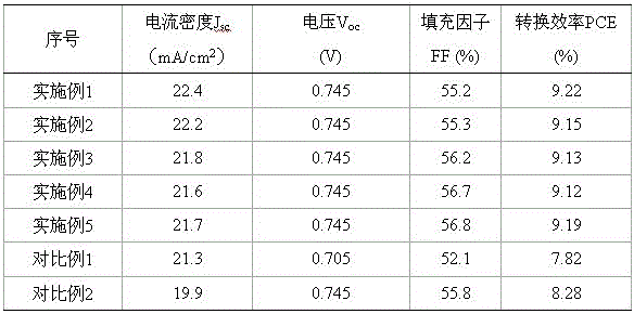
[0047] See Table 1 for the photoelectric performance test data of the polymer solar cell prepared by the above method.
Embodiment 3
[0049] Under nitrogen protection, a photoactive layer was prepared on the second hole transport layer. Au nanosheets with a thickness of 20nm and a side length of 50nm were doped into the semiconductor active material to prepare an active liquid with a weight content of 10%. Coating by spin coating, drying at room temperature for 30min, forming a photoactive layer film with a thickness of 150nm (the donor material in the semiconductor active material is PBDTTT-C-T, and the acceptor material is PC 71 BM), other preparation methods are the same as in Example 1.
[0050] See Table 1 for the photoelectric performance test data of the polymer solar cell prepared by the above method.
PUM
| Property | Measurement | Unit |
|---|---|---|
| particle diameter | aaaaa | aaaaa |
| thickness | aaaaa | aaaaa |
| thickness | aaaaa | aaaaa |
Abstract
Description
Claims
Application Information
 - R&D
- Intellectual Property
- Life Sciences
- Materials
- Tech Scout
- Unparalleled Data Quality
- Higher Quality Content
- 60% Fewer Hallucinations
Browse by: Latest US Patents, China's latest patents, Technical Efficacy Thesaurus, Application Domain, Technology Topic, Popular Technical Reports.
© 2025 PatSnap. All rights reserved.Legal|Privacy policy|Modern Slavery Act Transparency Statement|Sitemap|About US| Contact US: help@patsnap.com


