High Voltage Semiconductor Components

A semiconductor and component technology, applied in the field of high-voltage semiconductor components, can solve problems such as inability to apply high-voltage environments, and achieve the effect of improving high-voltage bearing capacity and meeting ultra-high-voltage requirements

Active Publication Date: 2017-07-18
UNITED MICROELECTRONICS CORP
View PDF5 Cites 0 Cited by
  • Summary
  • Abstract
  • Description
  • Claims
  • Application Information

AI Technical Summary

Problems solved by technology

[0003] However, the breakdown voltage of current MOSFET components is less than about 100 volts (volt, V), so they cannot be used in high-voltage environments or ultra-high-voltage environments with voltages as high as 500V to 1200V.

Method used


Image

  • High Voltage Semiconductor Components
  • High Voltage Semiconductor Components
  • High Voltage Semiconductor Components

Examples


Embodiment Construction

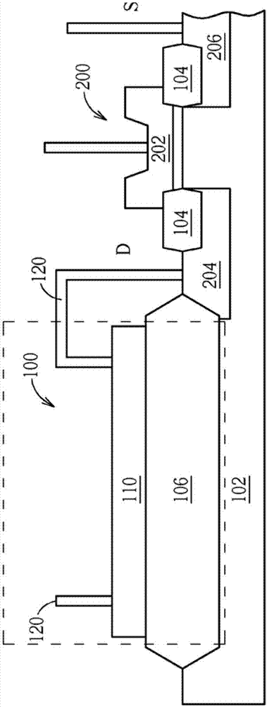
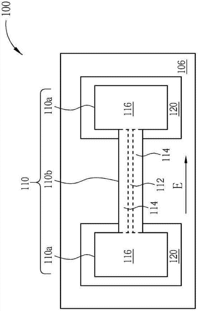
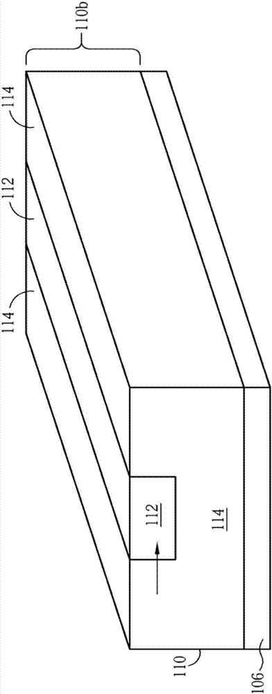
[0019] see figure 1 and image 3 , figure 1 and image 3 A schematic diagram of a first preferred embodiment of the high-voltage semiconductor element provided by the present invention, wherein figure 2 for figure 1 The top view of the high-voltage semiconductor components shown in the dotted line box, while image 3 for figure 2 A partially enlarged schematic diagram of a high-voltage semiconductor component. Such as figure 1 and figure 2 As shown, the high-voltage semiconductor device 100 provided by this preferred embodiment includes a substrate 102, and the substrate 102 may include different components required by integrated circuits, such as a MOS transistor device 200, and the MOS transistor device 200 may be a regular high voltage MOS transistor device or a high voltage MOS transistor device. And the MOS transistor device 200 may include a gate 202 , a first doped region 204 , and a second doped region 206 . The first doped region 204 and the second do...


PUM


Abstract

The invention discloses a high-voltage semiconductor element, which comprises a substrate, an insulating layer arranged on the substrate, and a silicon layer arranged on the insulating layer. The silicon layer further includes at least a first strip-shaped doped region, two-terminal doped regions respectively disposed at two ends of the silicon layer and electrically connected to the first strip-shaped doped region, and a plurality of second strip-shaped doped regions Doping regions, and the plurality of second strip-shaped doping regions are alternately arranged with the first strip-shaped doping regions. The first strip-shaped doped region and the plurality of terminal doped regions include a first conductivity type, the plurality of second strip-shaped doped regions include a second conductivity type, and the first conductivity type and The second conductivity type is complementary.

Description

technical field [0001] The present invention relates to a high-voltage semiconductor device, in particular to a high-voltage semiconductor device that can be integrated with a metal-oxide-semiconductor (MOS) transistor device. Background technique [0002] A transistor device is an element used in a circuit to switch a switch or enhance an electronic signal. In the early development of solid-state electronic circuits, bipolar junction transistors (bipolar junction transistors, BJT) components were the main components. With the increasing demand for high-speed, low-cost, and small-size digital devices, modern integrated circuits are The main force is metal-oxide-semiconductor field transistor (MOSFET) components. [0003] However, the current breakdown voltage of the MOSFET device is less than about 100 volts (volt, V), so it cannot be applied in a high-voltage environment or an ultra-high voltage environment with a voltage as high as 500V to 1200V. Therefore, there is stil...

Claims


Application Information

Patent Timeline
Patent Type & Authority Patents(China)
IPC IPC(8): H01L29/06H01L29/36H01L27/02
Inventor 张堡安李庆民吴德源王智充李文芳徐尉伦
Owner UNITED MICROELECTRONICS CORP
Why Eureka
Try Eureka