Optical readout full-hollow focal plane array provided with thermal sink structures and manufacturing method thereof

A focal plane array and optical readout technology, applied in the field of semiconductors, can solve the problems that the pixel structure cannot work independently, cannot be transferred to the substrate in time, and cannot be effectively controlled by FPA, and achieves the elimination of thermal crosstalk, low cost, The effect of high yield

Active Publication Date: 2013-09-25
北京中科微投资管理有限责任公司
View PDF7 Cites 1 Cited by
  • Summary
  • Abstract
  • Description
  • Claims
  • Application Information

AI Technical Summary

Problems solved by technology

However, due to its fully hollowed-out feature, the energy of the pixel cannot be transferred to the substrate in time. It can only be transferred to the substrate through the supporting frame to the edge of the film on the one hand, and dissipated through heat radiation on the other hand, resulting in macroscopically, TEC cannot effectively control the temperature of FPA, making the temperature of the entire film uneven; from a microscopic point of view, the pixel structure that absorbs infrared radiation energy and heats up cannot transmit energy in time, and part of the energy is transmitted to other surrounding deformed pixels through the frame. On the pixel, other pixels are also deformed, resulting in thermal crosstalk, and the structure of each pixel cannot work independently

Method used


Image

  • Optical readout full-hollow focal plane array provided with thermal sink structures and manufacturing method thereof
  • Optical readout full-hollow focal plane array provided with thermal sink structures and manufacturing method thereof
  • Optical readout full-hollow focal plane array provided with thermal sink structures and manufacturing method thereof

Examples


Embodiment Construction

[0031] The present invention will be described in detail below in conjunction with the accompanying drawings and by taking specific implementations as examples. However, those skilled in the art should know that the present invention is not limited to the specific embodiments listed, as long as it conforms to the spirit of the present invention, it should be included in the protection scope of the present invention.

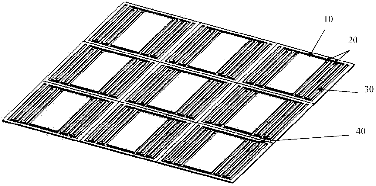
[0032] Such as figure 1 Shown is a three-dimensional schematic diagram of a single pixel of an opto-mechanical fully hollow focal plane array detector in the prior art, wherein each pixel includes a frame 40 and within the frame 40: a reflector 10, and two left and right The double-material deformed beam 20 is on the same plane as the two thermal isolation beams 30, the frame 40 and other components of the pixel.

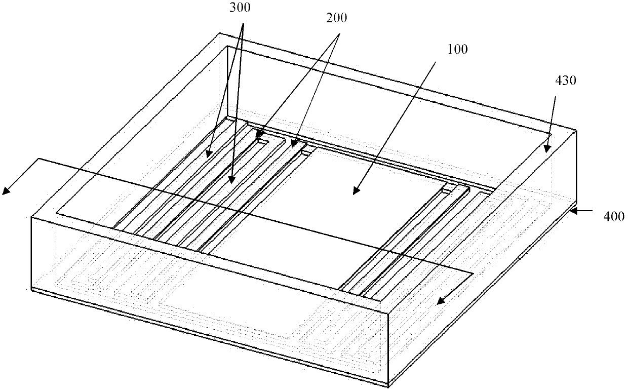
[0033] Such as figure 2 Shown is a three-dimensional schematic diagram of a single pixel unit of the optical readout full hollow focal plane array ...


PUM


Abstract

The invention discloses an optical readout full-hollow focal plane array provided with thermal sink structures and a manufacturing method thereof. Each pixel of the array comprises a framework and other parts such as a reflection board and the like in the framework, and the upper part of each pixel framework comprises a thermal sink structure formed by a thick metal film. The thermal sink structures enhance the thermal conductance of a whole film area and accelerate energy transmission, so that the temperature uniformity of the film area is improved greatly. A thermal crosstalk phenomenon caused by the fact that energy spreads along framework grids is eliminated, the response time is decreased, and the thermal imaging speed is accelerated. In addition, the thickness of a whole support framework is increased by 10 times, and the mechanical strength of the film area and the film smoothness are greatly improved. Besides, the frameworks tower above the plane where the parts of the pixels are in, so that reflection rays irradiated on the reflection boards can be separated from reflection rays irradiated on the frameworks, and imaging signals read by the reflection boards and reflection signals of the frameworks can be separated. The method is simple in process, short in production cycle and high in yield.

Description

technical field [0001] The invention belongs to the technical field of semiconductors, and in particular relates to an optical readout fully hollow focal plane array (Focal Plane Array, FPA) with a heat sink structure and a manufacturing method thereof. Background technique [0002] In the technical field of MEMS (Micro Electro Mechanical systems, micro-electro-mechanical systems), infrared detectors have been widely used in medical, industrial, military, commercial, scientific research and other fields. Usually can be divided into photoelectric infrared detectors and thermal infrared detectors. Photoelectric infrared detectors have the characteristics of fast response time and low noise equivalent temperature difference (Noise Equivalent Temperature Difference, NETD). Middle), resulting in large volume, high power consumption, and high price of this kind of infrared detector, which limits its development to civilian use. [0003] In recent years, uncooled infrared detecto...

Claims


Application Information

Patent Timeline
Patent Type & Authority Applications(China)
IPC IPC(8): B81B7/04B81C1/00
Inventor 刘瑞文焦斌斌陈大鹏
Owner 北京中科微投资管理有限责任公司
Why Eureka
Try Eureka