Method for flattening output spectra of arrayed waveguide grating
An arrayed waveguide grating and flattening technology, applied in optics, optical components, instruments, etc., can solve the problems of narrow 3dB bandwidth, demodulation performance affected by temperature changes and wavelength drift, and achieve high design freedom, low cost, and structural design simple effects
- Summary
- Abstract
- Description
- Claims
- Application Information
AI Technical Summary
Problems solved by technology
Method used
Image
Examples
Embodiment Construction
[0019] The best embodiment of the present invention will be described in detail below in conjunction with technical solutions and accompanying drawings.
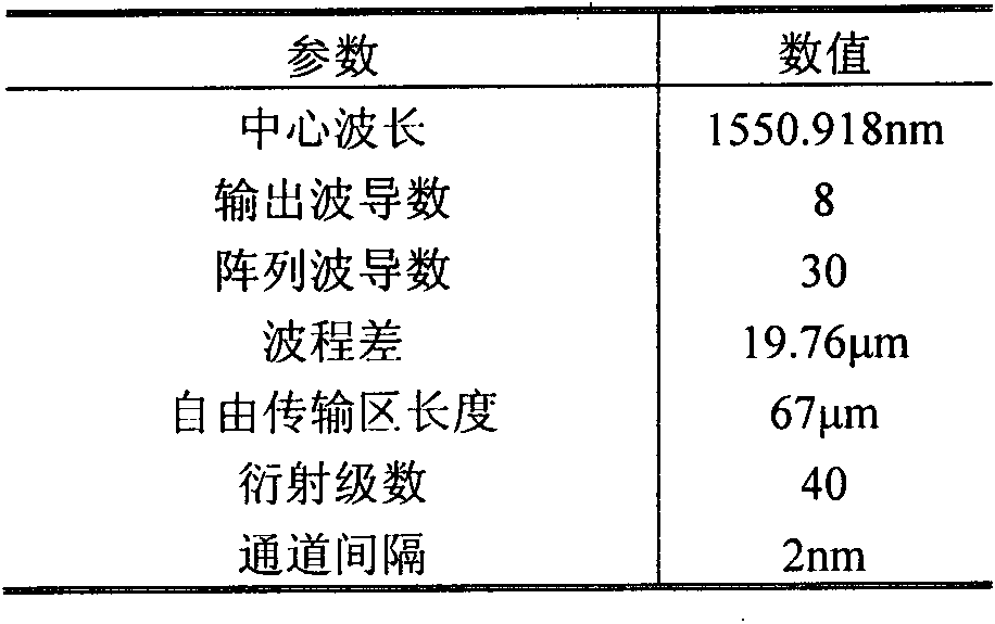
[0020] The structure schematic diagram of the arrayed waveguide grating output spectrum flattening method proposed by the present invention is as attached figure 1 shown. A tapered multimode waveguide structure is inserted before the input slab waveguide of the arrayed waveguide grating, and its optimal design parameters include the exit distance W O , entrance width W I , length L MMI and cone angle a. In order to increase design freedom and reduce crosstalk, a tapered waveguide is inserted before the tapered multimode waveguide and after the arrayed waveguide grating output slab waveguide, with a width of w i and w o .
[0021] According to the above structural analysis, the two structural parts of the planarization method are the tapered multimode waveguide part and the two tapered pre-broadening parts.
[0022] 1....
PUM
 Abstract
Description
Claims
Application Information
 - R&D
- Intellectual Property
- Life Sciences
- Materials
- Tech Scout
- Unparalleled Data Quality
- Higher Quality Content
- 60% Fewer Hallucinations
Browse by: Latest US Patents, China's latest patents, Technical Efficacy Thesaurus, Application Domain, Technology Topic, Popular Technical Reports.
© 2025 PatSnap. All rights reserved.Legal|Privacy policy|Modern Slavery Act Transparency Statement|Sitemap|About US| Contact US: help@patsnap.com


