
Method for manufacturing WOLED (White Organic Light Emitting Diode), WOLED and display equipment

An organic and light-emitting unit technology, applied in semiconductor/solid-state device manufacturing, semiconductor devices, electrical components, etc., and can solve problems affecting the quality of display devices, light leakage from WOLED displays, and product color mixing.

Active Publication Date: 2013-08-28
GUANGDONG JUHUA PRINTING DISPLAY TECH CO LTD
View PDF6 Cites 38 Cited by
  • Summary
  • Abstract
  • Description
  • Claims
  • Application Information

AI Technical Summary

Problems solved by technology

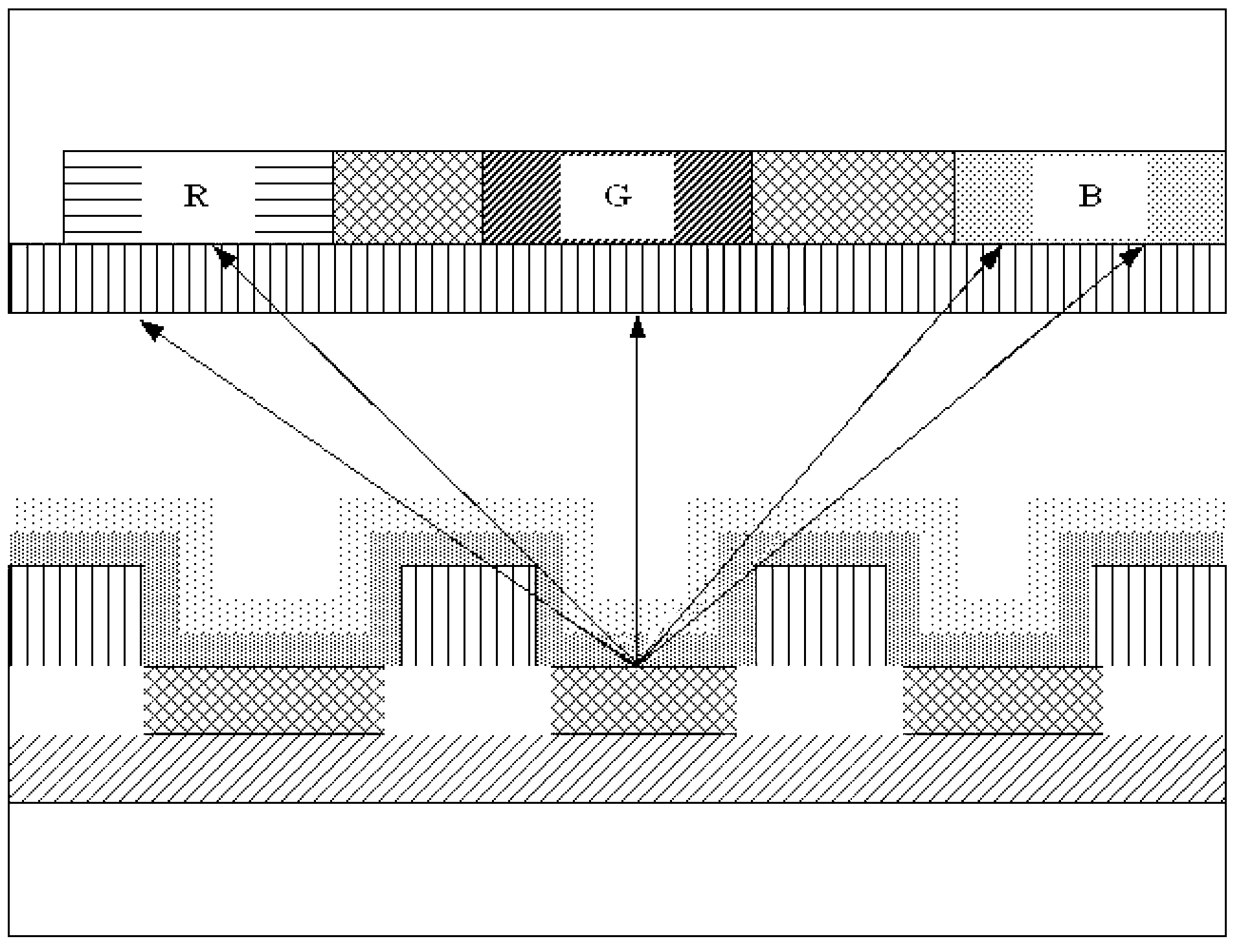
[0004] In the prior art, when laminating the TFT array substrate and the CF layer, there will be a gap of a certain value between the CF layer and the WOLED light-emitting layer, and because the WOLED light-emitting layer has the characteristics of a self-luminous light source, such as figure 1 As shown, when the light emitted by the organic light-emitting unit reaches the color filter substrate in the lateral direction, the gap will cause the manufactured WOLED display to leak laterally, resulting in color mixing of the product, thereby affecting the quality of the display device.

Method used


Image

  • Method for manufacturing WOLED (White Organic Light Emitting Diode), WOLED and display equipment
  • Method for manufacturing WOLED (White Organic Light Emitting Diode), WOLED and display equipment
  • Method for manufacturing WOLED (White Organic Light Emitting Diode), WOLED and display equipment

Examples


Embodiment Construction

[0021] Aiming at the problem of light leakage in the WOLED display in the prior art, which makes the image display quality of the display device poor, the technical solution proposed here in the embodiment of the present invention deposits a reflective metal thin film on the array substrate, so that the array substrate and the color After the lamination process of the film substrate, even if there is a gap, the deposited reflective metal film can reflect back the light source emitted by the WOLED light-emitting layer, which better avoids the color mixing problem caused by the lateral light leakage phenomenon of the WOLED display in the prior art. The display quality of the WOLED display is better improved.

[0022] The main realization principles, specific implementation methods and corresponding beneficial effects of the technical solutions of the embodiments of the present invention will be described in detail below with reference to each accompanying drawing.

[0023] Embod...


PUM

PropertyMeasurementUnit
Thicknessaaaaaaaaaa

Abstract

The invention discloses a method for manufacturing a WOLED (White Organic Light Emitting Diode), the WOLED and display equipment. The method comprises the following steps: forming an array substrate comprising an anode array on a substrate based on a composition process and forming a color filter substrate based on the composition process, including depositing a transparent organic thin film and a reflective metal thin film on the array substrate in sequence; patterning the reflective metal thin film to remove a metal thin film above an anode electrode; etching the transparent organic thin film by taking the patterned metal thin film as a mask to expose the anode electrode so as to form a pixel definition pattern; evaporating an organic light emitting unit and a cathode on the array substrate on which the pixel definition pattern is formed in sequence; and attaching the array substrate comprising the organic light emitting unit and the cathode with the color filter substrate to form the WOLED. According to the method, the light leakage phenomenon of the WOLED existing in the prior art can be avoided better, and the image display quality of the display equipment is improved.

Description

technical field [0001] The present invention relates to the field of display technology, in particular to a method for manufacturing a white organic light emitting diode (WOLED, White Organic Light Emitting Diode), a WOLED and a display device. Background technique [0002] With the vigorous development of flat-panel display technology, organic light-emitting diodes (OLED, Organic Light Emitting Diode) compared with traditional liquid crystal displays (LCD, Liquid Crystal Display), in addition to being thinner, more self-illuminating, low power consumption, no need Excellent features such as backlight, no viewing angle limitation, and high response rate have become the mainstream of the next-generation flat-panel display technology. [0003] In order to realize the full color of the OLED display, one way is to achieve it by superimposing a white organic light emitting diode (WOLED, White Organic Light Emitting Diode) and a color filter layer (CF, ColorFilter). Among them, t...

Claims


Application Information

Patent Timeline
IPC IPC(8): H01L51/56H01L51/52H01L27/32
Inventor 熊志勇赵本刚
Owner GUANGDONG JUHUA PRINTING DISPLAY TECH CO LTD
Learn More