
Beam splitting device and multi-beam interference light path system

A multi-beam interference and optical path system technology, applied in the field of micro-nano manufacturing and optical design, can solve the problems of expensive equipment, difficult photonic crystal structure, not compact, etc., and achieve adjustable beam splitting effect, simple overall structure and simple structure Effect

Inactive Publication Date: 2013-08-28
SUZHOU UNIV +1
View PDF3 Cites 2 Cited by
  • Summary
  • Abstract
  • Description
  • Claims
  • Application Information

AI Technical Summary

Problems solved by technology

Electron beam direct writing is not suitable for large-area production of photonic crystal structures due to expensive equipment and low efficiency; high-end miniature projection exposure machine equipment is also very expensive, and the production investment is relatively large; nanoimprint technology is still immature, and large-area It is difficult to make a photonic crystal structure; holographic exposure technology can produce a photonic crystal structure in a large area, at low cost, and relatively quickly
[0004] In the holographic interference exposure technology, if it is necessary to obtain a photonic crystal with a two-dimensional structure at one time, three beams or multi-beam interference exposure is required. The traditional method of splitting light through mirrors and semi-transparent mirrors is used to obtain multi-beam interference exposure. The optical path Very complex, and the optical path is large and not compact

Method used


Image

  • Beam splitting device and multi-beam interference light path system
  • Beam splitting device and multi-beam interference light path system
  • Beam splitting device and multi-beam interference light path system

Examples


Embodiment Construction

[0024] As mentioned in the background technology, the existing two-dimensional photonic crystal manufacturing method mainly adopts two methods. The first is to perform two or three exposures with double beams, and the second is to perform single exposure with more than three beams of light. exposures. For the first method, in the process of multiple exposures, precise position alignment is required for the two exposures before and after, so as to ensure that the two exposures before and after are carried out in the same area, so that the interference fringes are superimposed to form an interference lattice. Two-dimensional photonic crystal structure. However, this high-precision alignment has strict requirements on the mechanical operation part of the exposure machine. The movement error between each exposure is only allowed at the micron or even sub-micron level. To achieve this alignment requires a high-precision moving workpiece table. Undoubtedly, it brings a cost burden ...


PUM


Abstract

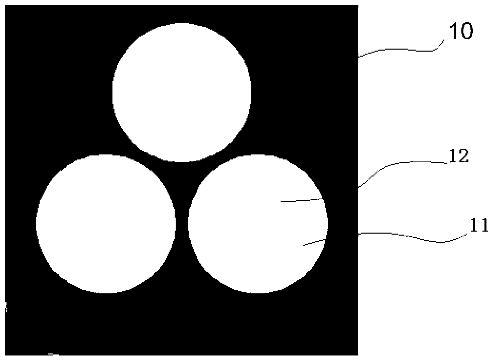
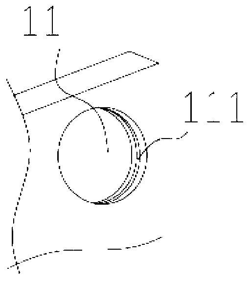
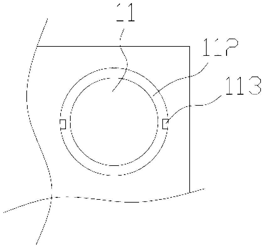
The invention discloses a beam splitting device and a multi-beam interference light path system. The beam splitting device comprises a light blocking mother board, multiple round holes formed in the light blocking mother board, and multiple beam splitting lenses positioned in the multiple round holes. The multiple beams are split through the multiple beam splitting lenses, and the beam splitting device has the advantages of simple principle and adjustable beam splitting effect; and moreover, the generated beam splitting light path is not required to be adjusted by employing multiple branches, so that the multi-beam interference light path system is simple and compact in overall structure and brings novel application prospects to multi-beam interference exposure.

Description

technical field [0001] The invention relates to an interference optical path system capable of making photonic crystals, especially an optical path system capable of three-beam or even multi-beam interference, and the interference angle is continuously adjustable. It involves the fields of micro-nano manufacturing and optical design. Background technique [0002] Photonic Crystal was independently proposed by S.john and E.Yablonovitch in 1987. It is an artificial microstructure formed by periodic arrangement of media with different refractive indices. Among the technologies used to manufacture high-power blue LEDs, the method of using photonic crystals to improve the luminous efficiency of LEDs is being increasingly proposed. The result of making photonic crystals on sapphire substrates can not only improve the external quantum efficiency of LEDs, but also effectively improve the lattice mismatch problem of GaN grown on sapphire substrates, such as the work of Y.K.Su et al....

Claims


Application Information

Patent Timeline
IPC IPC(8): G02B27/12
Inventor 袁晓峰陈林森浦东林
Owner SUZHOU UNIV
Learn More