Crosspoint-type variable-esistance non-volatile storage device

A non-volatile storage, resistance change technology, applied in information storage, static storage, digital storage information, etc., to achieve the effect of easy manufacturing and high practical value

Active Publication Date: 2013-08-07
PANASONIC SEMICON SOLUTIONS CO LTD
View PDF11 Cites 3 Cited by
  • Summary
  • Abstract
  • Description
  • Claims
  • Application Information

AI Technical Summary

Problems solved by technology

[0017] However, in the prior art described above, the resistance memory elements (resistance change elements) are arranged in the same order in the direction perpendicular to the semiconductor substrate in each layer so as to stabilize the characteristics of each layer during formation. In the case of a multi-layer cross-point type resistance change nonvolatile memory device composed of the first electrode, the resistance change layer, and the memory cell of the second electrode, it is difficult to use a unified current limiting method for each layer The problem of stabilizing the memory cell and performing the resistance change operation

Method used


Image

  • Crosspoint-type variable-esistance non-volatile storage device
  • Crosspoint-type variable-esistance non-volatile storage device
  • Crosspoint-type variable-esistance non-volatile storage device

Examples


reference example 1

[0163] [Description of circuit structure]

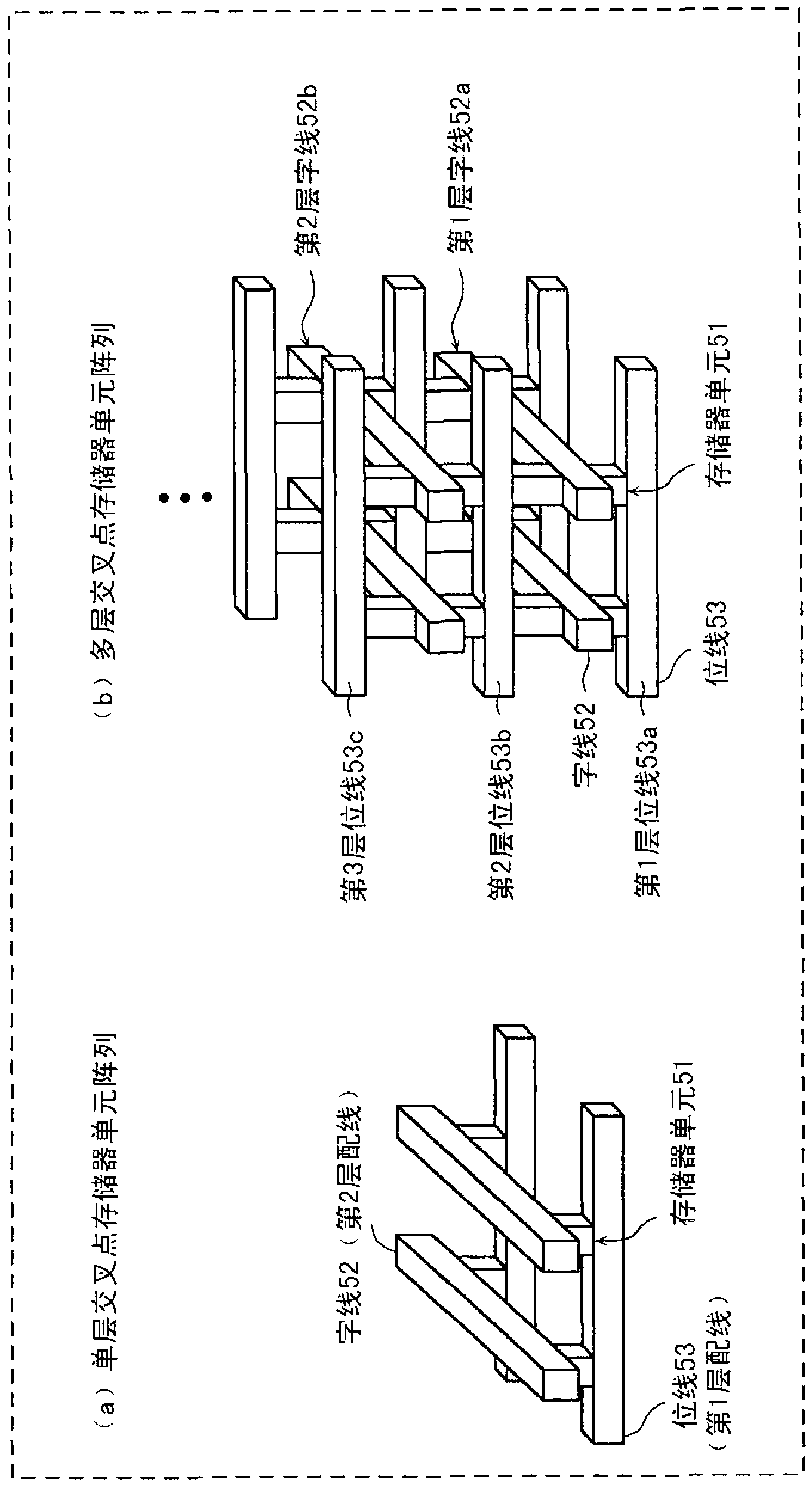
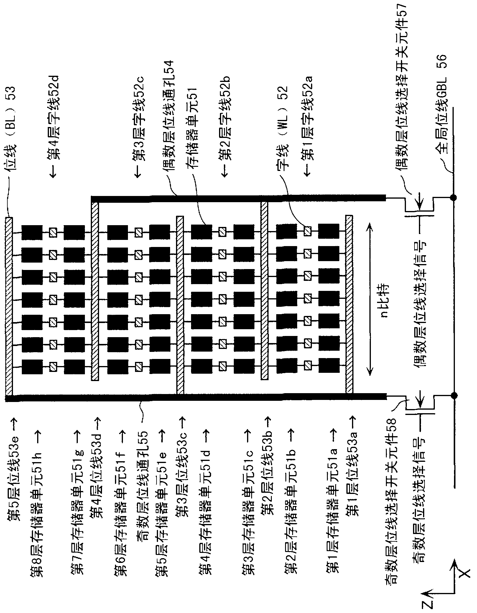
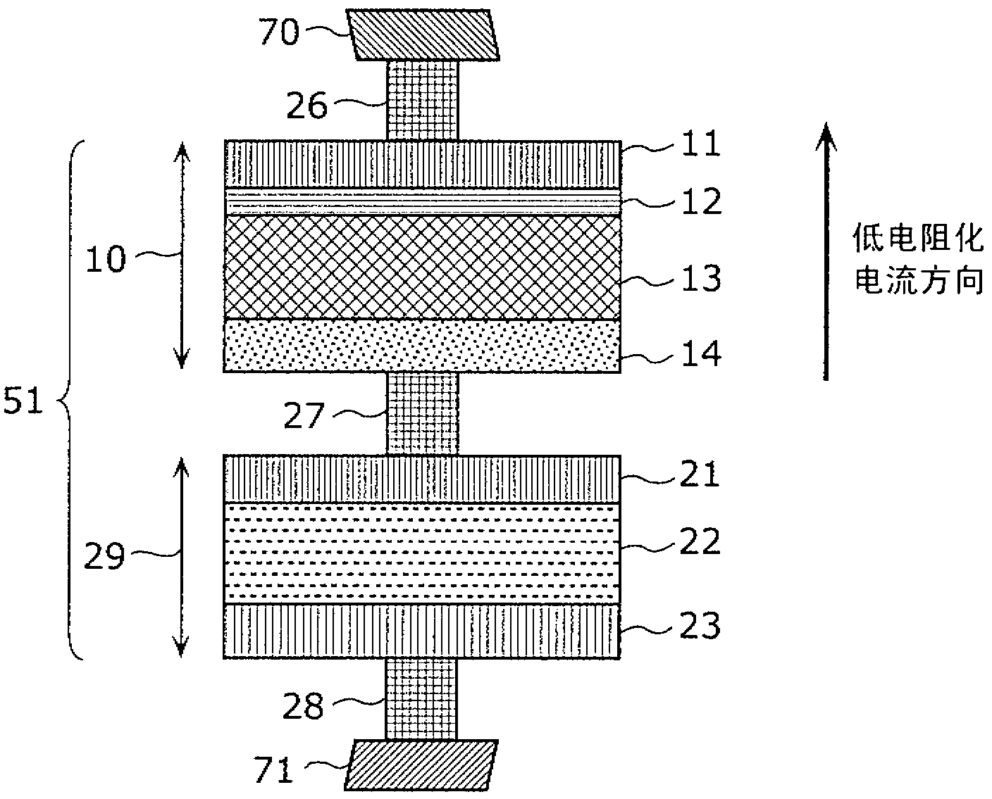
[0164] Picture 10 This is a diagram showing a cross-sectional structure of a memory cell 51 that constitutes a cross-point variable resistance nonvolatile memory device of a memory cell array with a multilayer structure of Reference Example 1.

[0165] The memory cell 51 has a structure in which the following elements are sequentially stacked: a first electrode 23 made of tantalum nitride (TaN); a current control layer 22 made of nitrogen-deficient silicon nitride; a second electrode 21 made of TaN; Use oxygen-deficient tantalum oxide (TaO x ) The first variable resistance layer 13 constituted; it is formed by oxidizing the first variable resistance layer 13 in an oxygen plasma atmosphere, and the oxygen deficiency is less than TaO x TaO y (X <y) A second variable resistance layer 12 composed of; and a third electrode 11 composed of platinum (Pt). A lower wiring 71 made of aluminum (Al) is arranged in the lower layer of the memory cell 5...

reference example 2

[0412] In Reference Example 1, in the writing operation to the nonvolatile memory device of the multi-layer cross-point structure, the following cases are described. Depending on the memory array layer to be written, the flow to the memory cells belonging to the memory array layer The direction of the current in the direction of lower resistance is to activate only the transistor of the current limiting element of the N-type current limiting element 90 or the P-type current limiting element 91, which produces a greater substrate bias effect, to perform a low-resistance operation, and reduce The current limit of resistive writing is the action mode of the source follower (ie, the source follower mode).

[0413] In Reference Example 2, it is assumed that the N-type current limiting element 90 and the P-type current limiting element 91 have the same structure, but the control method is different. Depending on the memory array layer to be written, a desired voltage is applied to the ...

Embodiment approach )

[0694] Hereinafter, embodiments of the present invention will be described in detail with reference to the drawings. In addition, the embodiments described below are all used to show a preferred specific example of the present invention. The numerical values, shapes, materials, components, arrangement positions and connection methods of components, steps, order of steps, etc. shown in the following embodiments are merely examples, and the gist of the invention is not limited. The present invention is limited only by the claims. Therefore, with regard to the constituent elements of the following embodiments, the constituent elements not described in the independent claims representing the highest concept of the present invention are not necessarily the constituent elements required to realize the subject of the present invention, but merely constitute more The components of the preferred mode are described.

[0695] In addition, in the following embodiments, the description will...


PUM


Abstract

Memory cells (51) are formed at each intersection between X-axis bit lines (53a and 53b) and Y-axis word lines (52a) formed in a plurality of layers. In a multi-layer crosspoint structure in which there is a plurality of vertical array surfaces sharing a word line arranged on the Y axis for every group of bit lines aligned with the Z axis, the even-numbered layer bit lines (53b) sharing a connection are connected and disconnected from a global bit line (56) by an even-numbered layer bit line-selecting switching element (1002), and the odd-numbered layer bit lines (53a) sharing a connection are connected and disconnected from the global bit line (56) by an odd-numbered layer bit line-selecting switching element (1001). The even-numbered layer bit line-selecting switching element (1002) and the odd-numbered layer bit line-selecting switching element (1001) have a bit line-selecting function and, during low-resistance writing, a current-limiting function.

Description

Technical field [0001] The present invention relates to a nonvolatile memory device having a cross-point type memory cell constructed using a so-called variable resistance element. Background technique [0002] In recent years, research and development of nonvolatile memory devices having memory cells constructed using so-called variable resistance elements have been advanced. The variable resistance element refers to an element that has a property that the resistance value changes (transitions between a high-resistance state and a low-resistance state) in response to an electrical signal, and can store information in accordance with the change in the resistance value. [0003] Also, regarding memory cells using variable resistance elements, one of them has a so-called cross point structure. In the cross point structure, each memory cell sandwiched between the bit line and the word line is formed at the position of the intersection of the bit line and the word line arranged orthog...

Claims


Application Information

Patent Timeline
Patent Type & Authority Applications(China)
IPC IPC(8): H01L27/105G11C13/00H01L27/10H01L45/00H01L49/00
CPCH01L27/2481H01L45/1233G11C2213/71G11C13/0007H01L27/2418G11C13/0023H01L45/08H01L45/146G11C13/0026G11C13/00G11C2213/77G11C13/0002G11C13/004G11C13/0069H10B63/22H10B63/84H10N70/24H10N70/826H10N70/8833
Inventor 东亮太郎岛川一彦
Owner PANASONIC SEMICON SOLUTIONS CO LTD
Why Eureka
Try Eureka