Improved AHB-to-APB bus bridge and control method thereof
A technology of APB bus and control method, which is applied in the direction of instruments, electrical digital data processing, etc., can solve the problems of not supporting two same-frequency bus operations, incompatible memory interfaces, etc., so as to avoid transmission operation errors, simplify circuit functions, and improve Effect of Transfer Operation Speed
- Summary
- Abstract
- Description
- Claims
- Application Information
AI Technical Summary
Problems solved by technology
Method used
Image
Examples
Embodiment 1
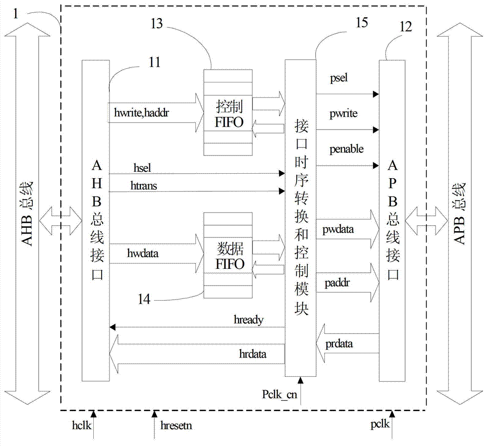
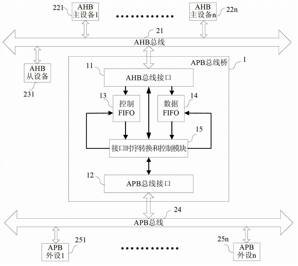
[0099] figure 1 A block diagram of the APB bus bridge in the embodiment of the present invention is described. The APB bus bridge 1 of the embodiment of the present invention includes: an AHB bus interface 11, an APB bus interface 12, a control FIFO 13, a data FIFO 14, and an interface timing conversion and control module 15. From figure 1 Among them, those in the professional field can clearly see the connection relationship between the transmission request signal of the AHB bus master and the APB bus bridge control signal, so as to understand the important technical features that constitute the technical solution of the present invention:
[0100] (1) The preparation signal hready output by the interface timing conversion and control module 15 is connected to the AHB bus interface 11, and the preparation signal hready is connected to the AHB master device connected to the AHB bus through the AHB bus interface 11.
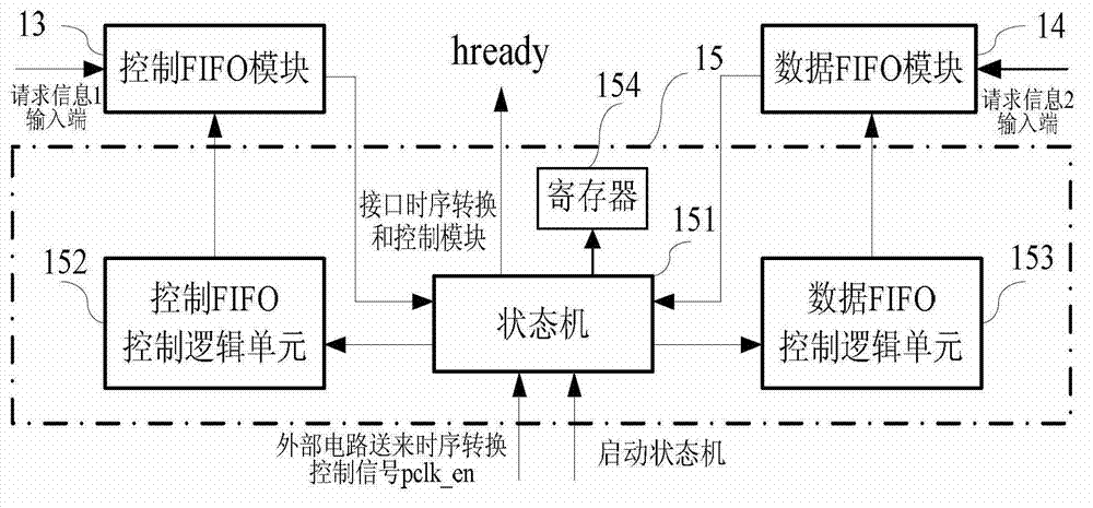
[0101] (2) The external circuit generates a timing tra...
Embodiment 1
[0133] Figure 5 Shown is a timing diagram of the continuous write transfer operation of the AHB bus in the case of an asynchronous clock between the AHB bus and the APB bus in the embodiment of the present invention. combine Figure 5 The example further illustrates the queue buffer control mechanism of the continuous write transmission in the embodiment of the present invention, which is an idea of speeding up the write transmission operation. Usually, considering the power consumption factor of the two buses, the APB bus clock pclk is slower than the AHB bus clock hclk, and the processing speed of the APB bus peripherals is relatively slow. Figure 5 The clock signals of the AHB bus and the APB bus given in are hclk and pclk respectively. The example sets the clock pclk as the frequency division of the clock hclk by two. The interface timing conversion signal pclk_en is formed by sampling the rising edge of the clock pclk. The waveform is the same as the clock pclk . E...
Embodiment 2
[0137] Figure 6 It is a sequence diagram of a single read transmission of AHB bus and APB bus asynchronous frequency multiplication of the present invention, such as Figure 6 As shown in , AHB bus and APB bus clock and timing conversion control signal and Figure 5same. Assume that before time T1, the request queues stored in the control FIFO module 13 and the data FIFO module 14 have all been read, and the storage status of the two FIFO modules is empty. Embodiment setting AHB bus master 221 is described as follows to the timing diagram of the single read transmission operation that APB bus peripheral 251 sends:
[0138] At time T1, the preparation signal hready output by the APB bus bridge is high level, and a master device 221 of the AHB bus sends a read transmission request, the read transmission request includes the read and write transmission signal hwrite is low level (ie read operation), and the destination for haddr1. At time T2, the APB bus bridge receives the ...
PUM
 Abstract
Description
Claims
Application Information
 - Generate Ideas
- Intellectual Property
- Life Sciences
- Materials
- Tech Scout
- Unparalleled Data Quality
- Higher Quality Content
- 60% Fewer Hallucinations
Browse by: Latest US Patents, China's latest patents, Technical Efficacy Thesaurus, Application Domain, Technology Topic, Popular Technical Reports.
© 2025 PatSnap. All rights reserved.Legal|Privacy policy|Modern Slavery Act Transparency Statement|Sitemap|About US| Contact US: help@patsnap.com


