Liquid crystal display panel and manufacture method thereof
The technology of a liquid crystal panel and a manufacturing method, which is applied in the field of manufacturing the liquid crystal panel, can solve problems such as lowered reliability of the liquid crystal panel, corrosion of the metal structure of the liquid crystal panel, and aggravated corrosion risk, so as to avoid reliability problems and uneven thickness problems , Reduce the effect of border light leakage
- Summary
- Abstract
- Description
- Claims
- Application Information
AI Technical Summary
Problems solved by technology
Method used
Image
Examples
Embodiment 1
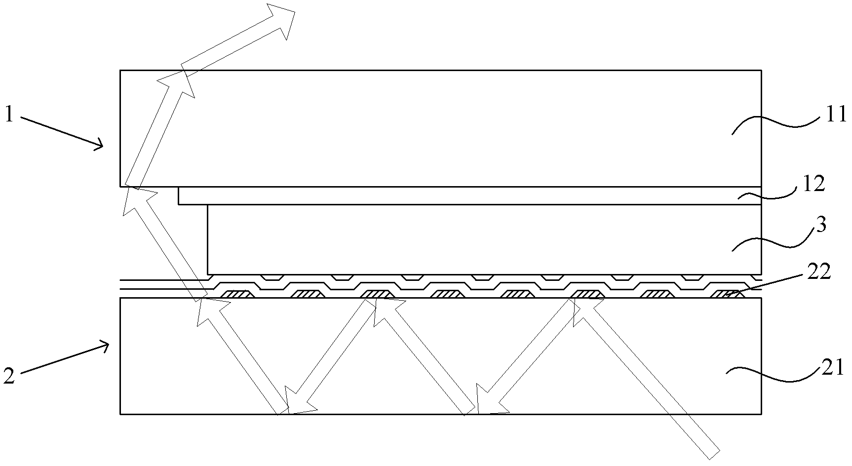
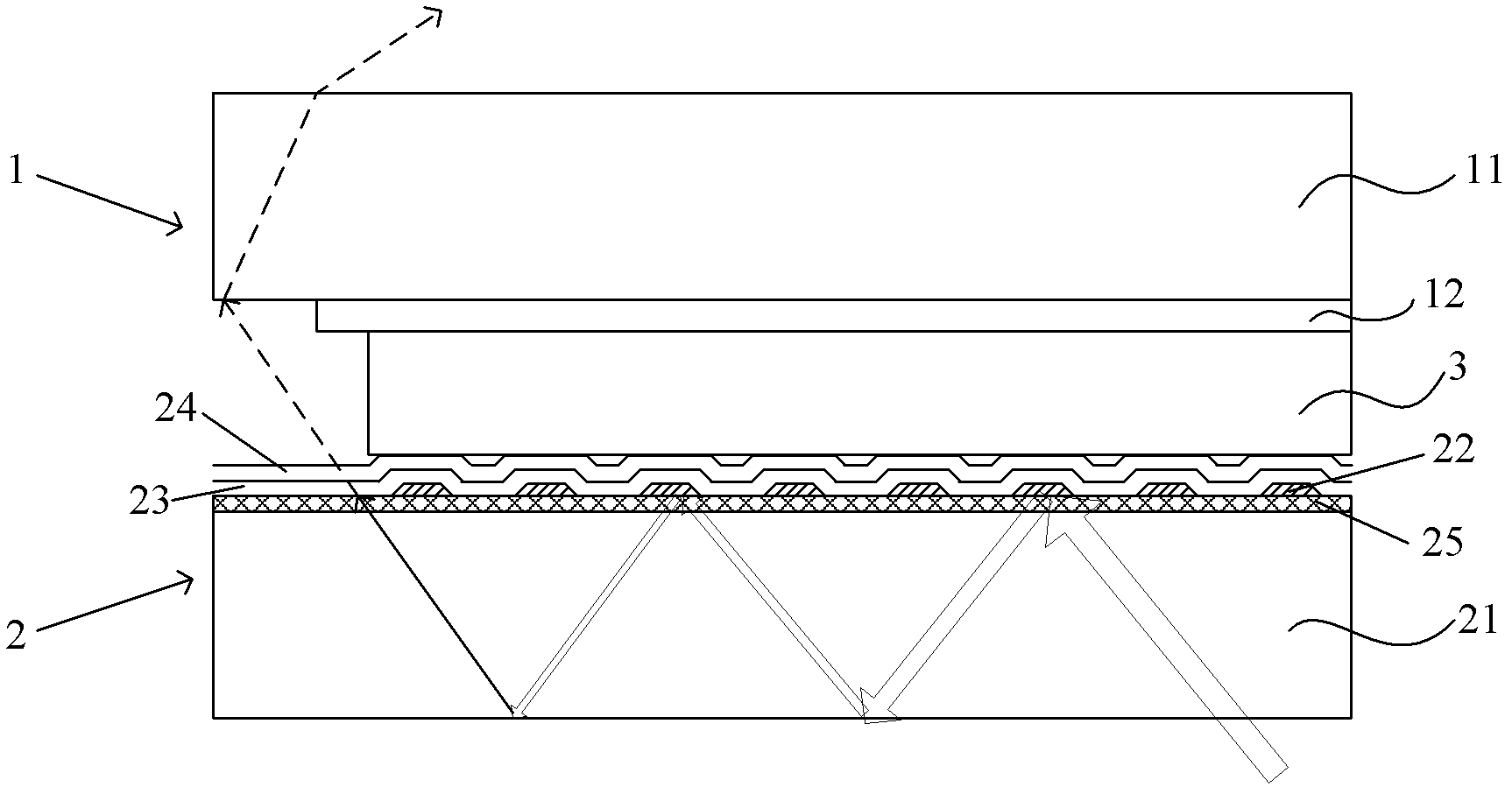
[0033] The liquid crystal panel in this embodiment includes a display area and a frame area surrounding the display area. figure 2 Shown is a schematic cross-sectional view of the frame area of the liquid crystal panel. As shown in the figure, the liquid crystal panel includes a color filter substrate 1 and an active device array substrate 2 , which are connected by a sealant 3 .
[0034] The color filter substrate 1 includes a base 11 and a black matrix 12 , while other structures of the color filter substrate 1 are not shown in the figure.
[0035] The active device array substrate 2 includes a base 21 , common electrode lines 22 , a transparent dielectric layer 23 and a transparent dielectric layer 24 , and both the transparent dielectric layer 23 and the transparent dielectric layer 24 can be made of, for example, silicon nitride. In the display area, a plurality of thin film transistors (not shown) are arranged on the substrate 21 . Wherein, the common electrode line...
Embodiment 2
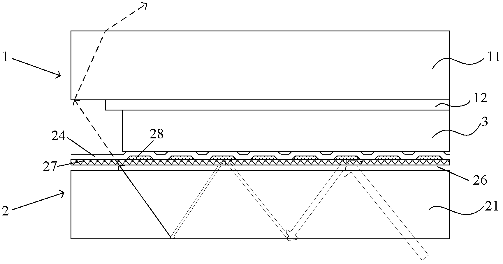
[0040] The liquid crystal panel in this embodiment also includes a display area and a frame area surrounding the display area. image 3 Shown is a schematic cross-sectional view of the frame area of the liquid crystal panel. In this embodiment, the substrate 11, the black matrix 12, the sealant 3, the transparent medium layer 24 and the substrate 21 are all the same as those in Embodiment 1, and in the display area, the substrate 21 There are also a plurality of thin film transistors (not shown in the figure), but the layer structure between the transparent medium layer 24 and the substrate 21 is different from that of the first embodiment.
[0041] In this embodiment, in the frame area, a transparent layer 26 , a light absorbing layer 27 , and common electrode lines 28 are on the substrate 21 in order, and the transparent medium layer 24 is on the common electrode lines 28 .
[0042] The transparent layer 26, the light-absorbing layer 27, and the common electrode line 28 r...
PUM
 Abstract
Description
Claims
Application Information
 - R&D
- Intellectual Property
- Life Sciences
- Materials
- Tech Scout
- Unparalleled Data Quality
- Higher Quality Content
- 60% Fewer Hallucinations
Browse by: Latest US Patents, China's latest patents, Technical Efficacy Thesaurus, Application Domain, Technology Topic, Popular Technical Reports.
© 2025 PatSnap. All rights reserved.Legal|Privacy policy|Modern Slavery Act Transparency Statement|Sitemap|About US| Contact US: help@patsnap.com


