
Look-up tables for delay circuitry in field programmable gate array (fpga) chipsets

A chipset and gate array technology, applied in logic circuits using specific components, logic circuits using basic logic circuit components, CAD circuit design, etc., can solve the problem of expensive FPGA units and achieve the effect of saving space and reducing costs

Inactive Publication Date: 2013-06-12
ERICSSON (CHINA) COMMUNICATION COMPANY LTD
View PDF5 Cites 5 Cited by
  • Summary
  • Abstract
  • Description
  • Claims
  • Application Information

AI Technical Summary

Problems solved by technology

In many designs, this clock speed is not needed without delay cells, and so such implementations often make FPGA cells more expensive

Method used


Image

  • Look-up tables for delay circuitry in field programmable gate array (fpga) chipsets
  • Look-up tables for delay circuitry in field programmable gate array (fpga) chipsets
  • Look-up tables for delay circuitry in field programmable gate array (fpga) chipsets

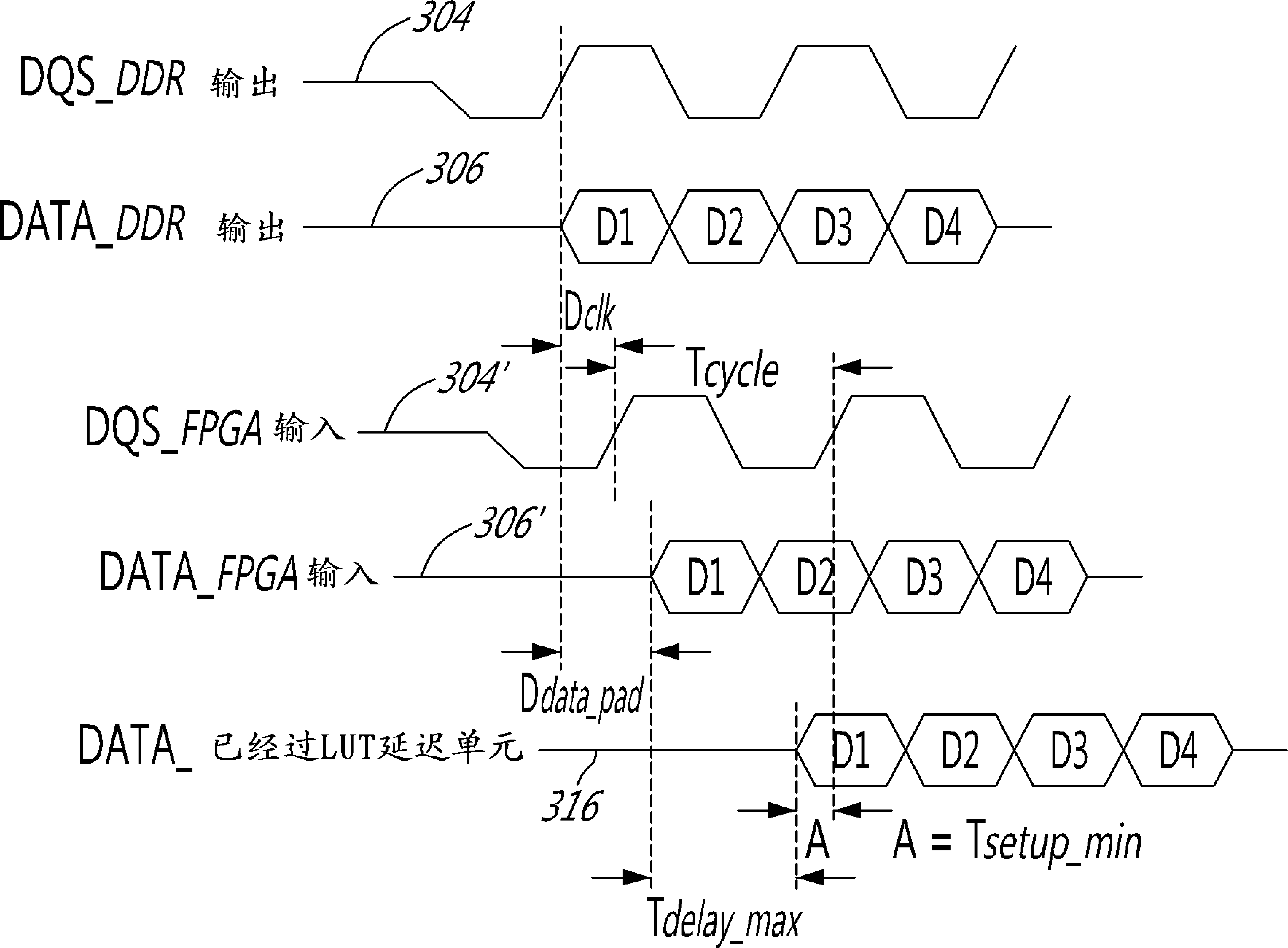
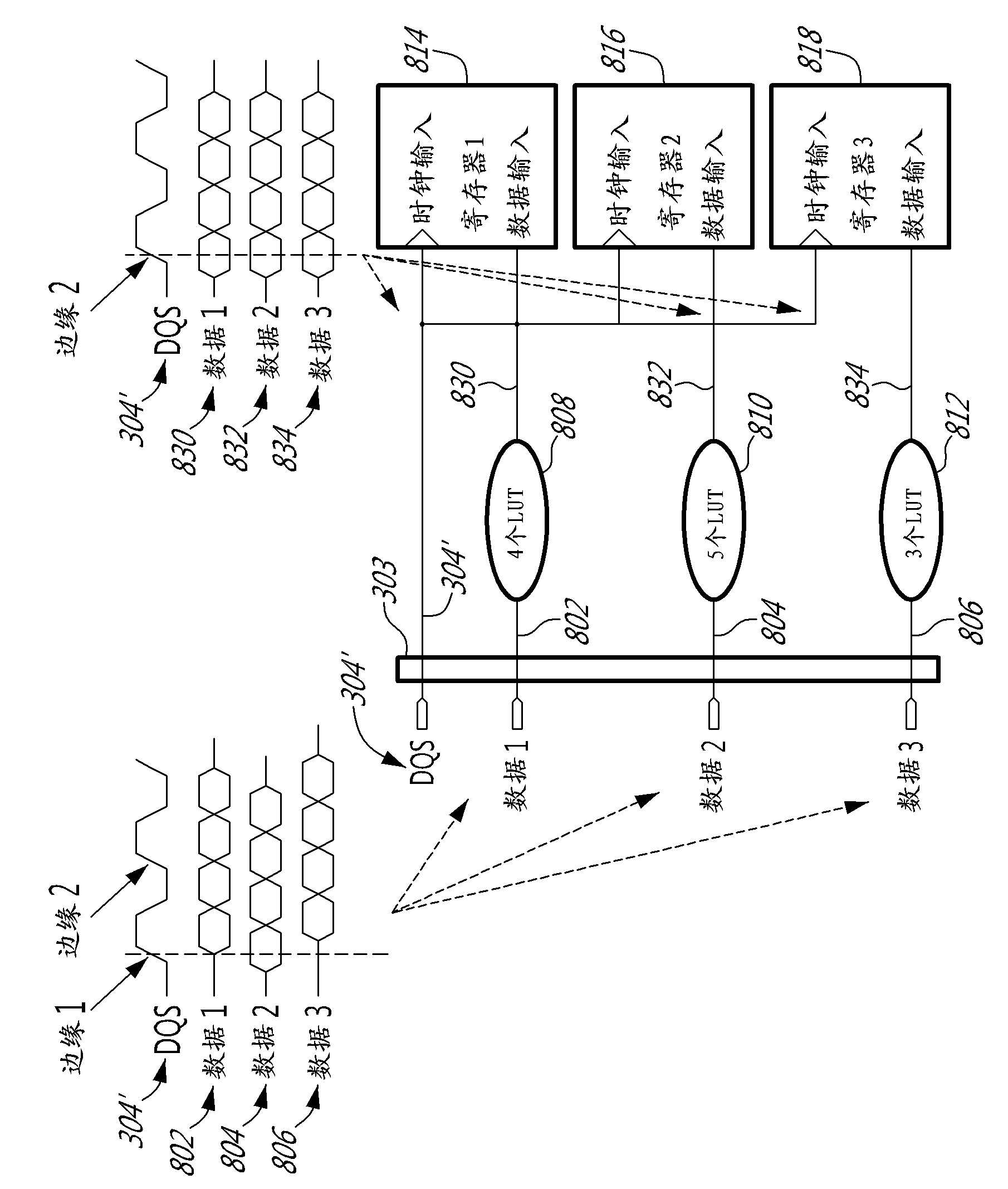
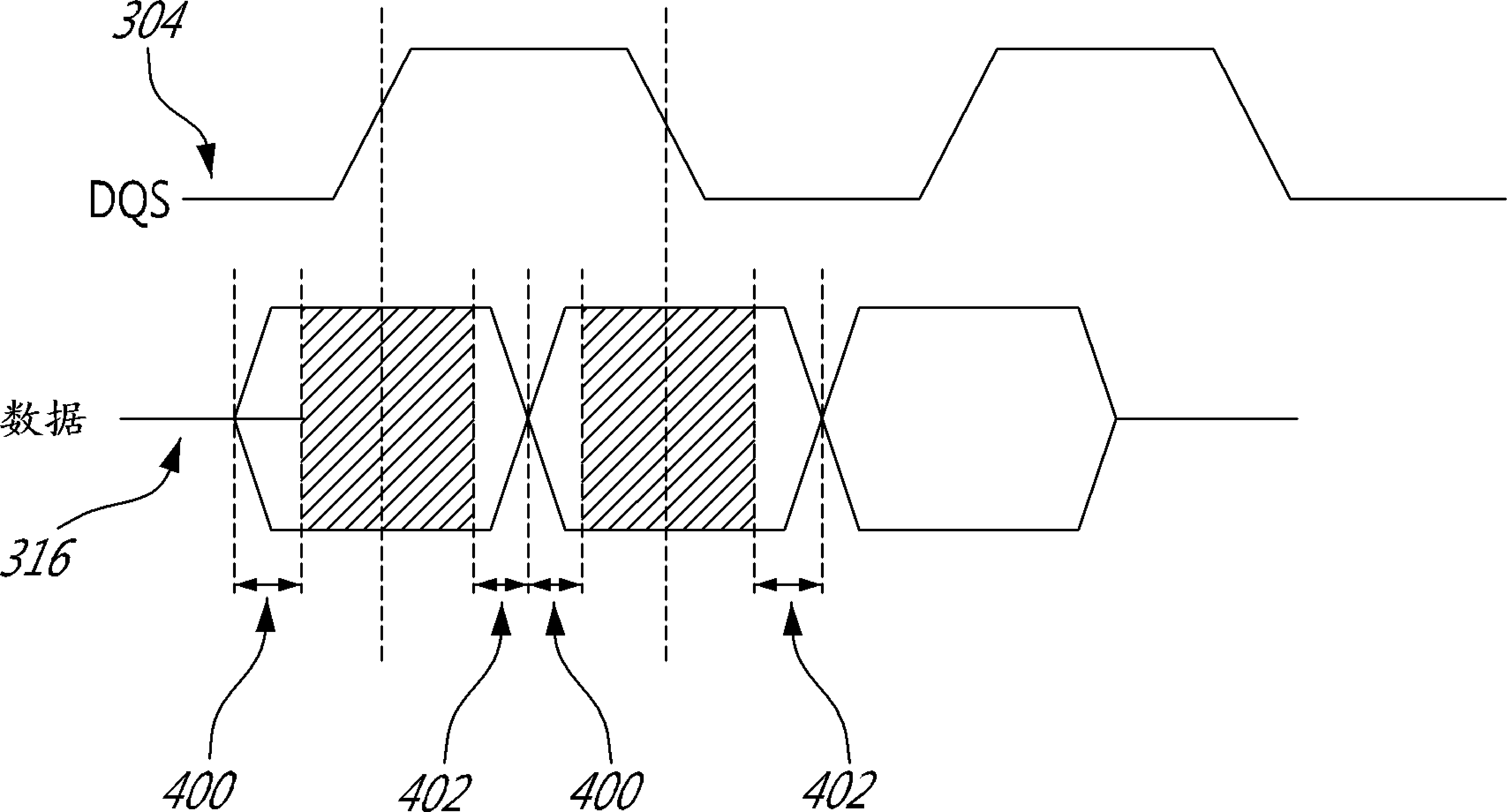
Examples


Embodiment Construction

[0023] The innovative teachings of the present invention will be described with particular reference to various exemplary embodiments. It should be understood, however, that this class of embodiments provides only a few examples of the many advantageous uses of the innovative teachings of the present invention. In general, statements made in the specification of the present application do not necessarily limit any of the various claimed aspects of the invention. Additionally, some statements may apply to some inventive features but not to others. In the drawings, like reference numerals are used throughout the several views to designate like or similar elements.

[0024] When the FPGA chipset samples the data signal, the phase relationship between the data signal and the corresponding clock signal must meet a series of requirements imposed by the FPGA chipset itself. If the data signal phase is not adjusted and somehow properly synchronized with the phase of the clock signal...


PUM


Abstract

A method, new use for Look-Up Tables (LUTs), and a Field Programmable Gate Array (FPGA) chipset are provided for delaying data signals. The FPGA comprises an input and a set of LUTs operationally connected to and receiving from the interface a data signal and a clock signal. The set of LUTs delay the data signal by a delay so that a corresponding first delayed data signal output from the set of LUTs is so synchronized with the clock signal for appropriate sampling of the delayed data signal to be performed by the FPGA chipset. A process of manufacturing of the FPGA chipset comprises calculating a delay for delaying and synchronising the data signal with a clock signal to meet requirements of the chipset, calculating a number of LUTs for delaying the data signal, and implementing in a data path of the data signal the number of LUTs.

Description

technical field [0001] The present invention relates to the field of Field Programmable Gate Array (FPGA) chipsets. Background technique [0002] A Field Programmable Gate Array (FPGA) is an integrated circuit designed to be configured by a customer or designer after manufacture. The FPGA configuration can be specified using a hardware description language (HDL), similar to the language used for application specific integrated circuits (ASICs). An FPGA can be used to implement any logic function that an ASIC can perform. The ability to update functionality after shipment, partial reconfiguration of parts of the design, and low incidental engineering costs relative to ASIC design (albeit generally higher unit costs) offer advantages for many applications. An FPGA contains programmable logic components called "logic blocks" and a hierarchy of reconfigurable interconnects that allow blocks to be "wired together", sort of like a reconfigurable interconnection of many (changeab...

Claims


Application Information

Patent Timeline
IPC IPC(8): H03K19/173
CPCG06F30/34H03K19/1731H03K19/17728
Inventor 曲克楠高同海
Owner ERICSSON (CHINA) COMMUNICATION COMPANY LTD
Learn More