High integration density display screen unit
A high-integration, display technology, applied in the direction of instruments, identification devices, etc., can solve the problems of complex LED box structure, complex assembly process, low assembly efficiency, etc., to simplify the production and installation process, convenient transportation process, and installation efficiency high effect
- Summary
- Abstract
- Description
- Claims
- Application Information
AI Technical Summary
Problems solved by technology
Method used
Image
Examples
Embodiment Construction
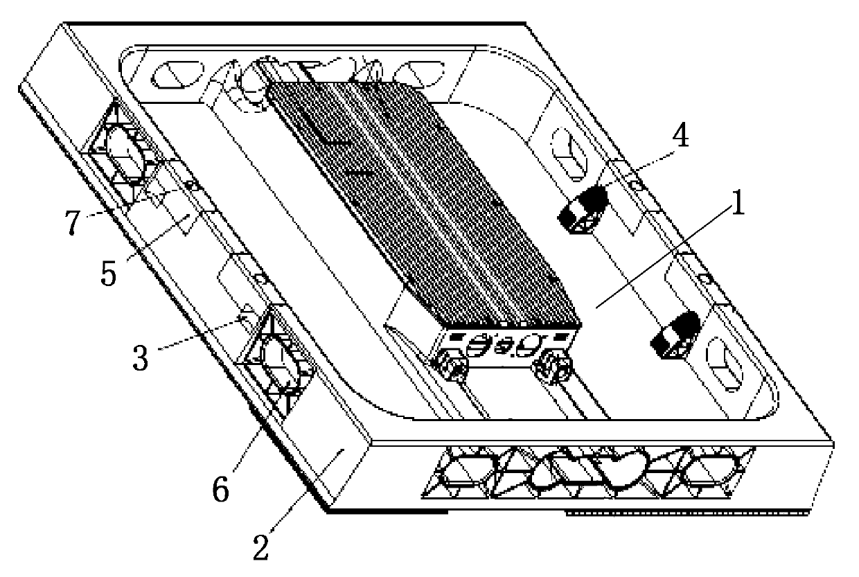
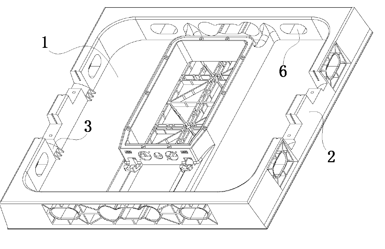
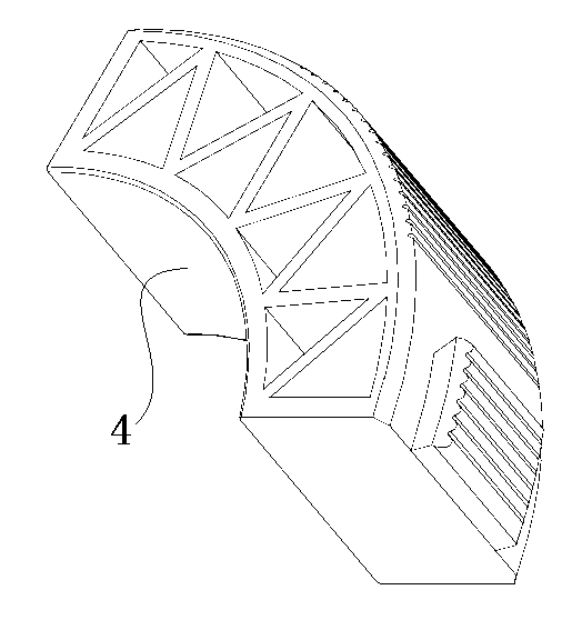
[0058] A highly integrated display unit such as figure 1 and 2 As shown, it includes a face shield 20, four PCB boards 10 of 249*249mm, and a display unit body 1 made of polymer nanomaterials. The back of the display unit body 1 is equipped with a connection board located in the control box 16 17. Receiving card 18, HUB and power supply 23. The control box is equipped with data signal transmission line 8 and power line 9. The front of the display unit main body 1 is directly connected to the PCB board 10 by screws. The PCB board 10 is fixed with face shield 20 by screw. Therefore, screw holes are provided on the front of the display unit main body 1, which can be used to directly fix the PCB 10. LED lights are arranged on the front of the PCB 10, and integrated chips are arranged on the back. Glue filling positions are reserved on the front of the PCB 10 and the main body of the display unit 1, that is, a process slot is set up around the kit on the front of the box body 1, ...
PUM
 Abstract
Description
Claims
Application Information
 - R&D
- Intellectual Property
- Life Sciences
- Materials
- Tech Scout
- Unparalleled Data Quality
- Higher Quality Content
- 60% Fewer Hallucinations
Browse by: Latest US Patents, China's latest patents, Technical Efficacy Thesaurus, Application Domain, Technology Topic, Popular Technical Reports.
© 2025 PatSnap. All rights reserved.Legal|Privacy policy|Modern Slavery Act Transparency Statement|Sitemap|About US| Contact US: help@patsnap.com


