Method for forming thin film solar cell with buffer-free fabrication process

A technology of solar cells and thin films, applied in sustainable manufacturing/processing, final product manufacturing, circuits, etc., can solve the problems of passive, unable to provide sidewalls, etc., to achieve high energy output and increase solar energy conversion efficiency.

Active Publication Date: 2013-05-15
TAIWAN SEMICON MFG CO LTD
View PDF4 Cites 2 Cited by
  • Summary
  • Abstract
  • Description
  • Claims
  • Application Information

AI Technical Summary

Problems solved by technology

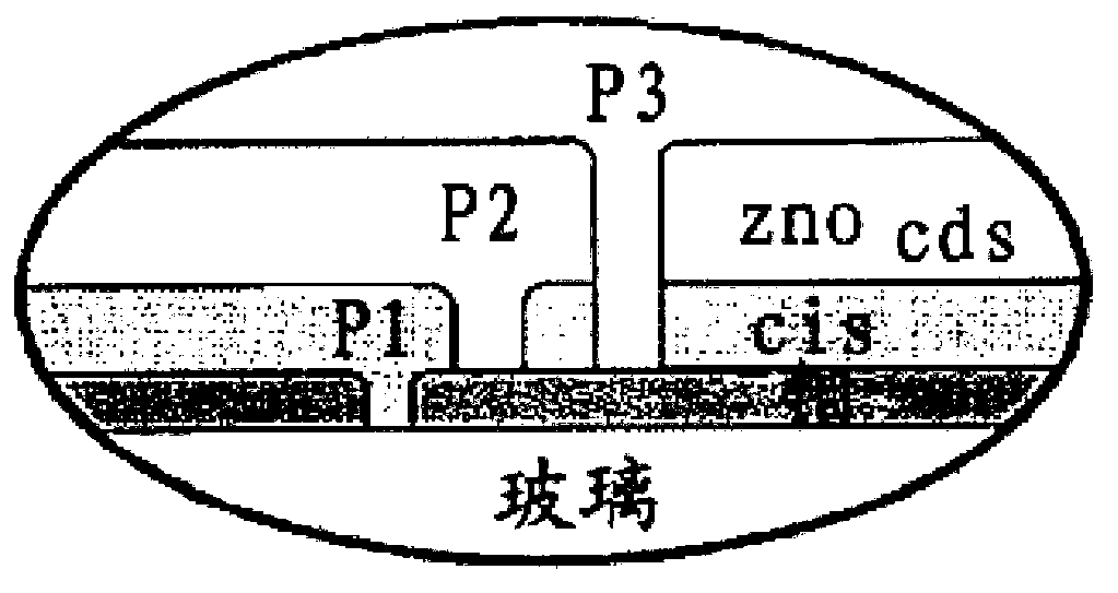
As shown in Figure 1B, although the material from the top TCO electrode layer extends down through the P2 scribe, the vertical walls of the P2 scribe still do not provide a good interface and make the sidewalls essentially passive for current collection. High quality active n-p junction
This limits the current density, power output potential, and efficiency of such thin-film solar cells with only the top CdS buffer layer above the absorber layer.

Method used


Image

  • Method for forming thin film solar cell with buffer-free fabrication process
  • Method for forming thin film solar cell with buffer-free fabrication process
  • Method for forming thin film solar cell with buffer-free fabrication process

Examples


Embodiment Construction

[0043] This illustrative description is intended to be read in conjunction with the accompanying drawings, which are to be considered a part of this entire specification. In the description of the embodiments disclosed herein, any expression of direction or orientation is merely for convenience of description, and is not intended to limit the scope of the present invention in any way. Related terms such as "lower", "upper", "horizontal", "vertical", "above", "below", "upper", "lower", "top", and "bottom" and their Variations of (eg, "horizontally," "downwardly," "upwardly," etc.) should be understood to refer to orientations as described thereafter or as shown in the figures in the discussion. These relative terms are for convenience of description only and do not require that the device be constructed or operated in a particular orientation. Unless otherwise stated, terms such as "attached," "mounted," "connected," and "interconnected" refer to a relationship in which struct...


PUM


Abstract

The invention provides a method for forming a thin film solar cell with buffer-free fabrication process, particularly a thin film solar cell and process for forming the same. The solar cell includes a bottom electrode layer, a light absorbing semiconductor layer, and top electrode layer. The absorber layer includes a p-type interior region and an n-type exterior region formed around the perimeter of the layer from a modified native portion of the p-type interior region, thereby forming an active n-p junction that is an intrinsic part of the absorber layer. The top electrode layer is electrically connected to the bottom electrode layer via a scribe line formed in the absorber layer that defines sidewalls. The n-type exterior region of the absorber layer extends along both the horizontal top of the absorber layer, and onto the vertical sidewalls of the scribe line to increase the area of available n-p junction in the solar cell thereby improving solar conversion efficiency.

Description

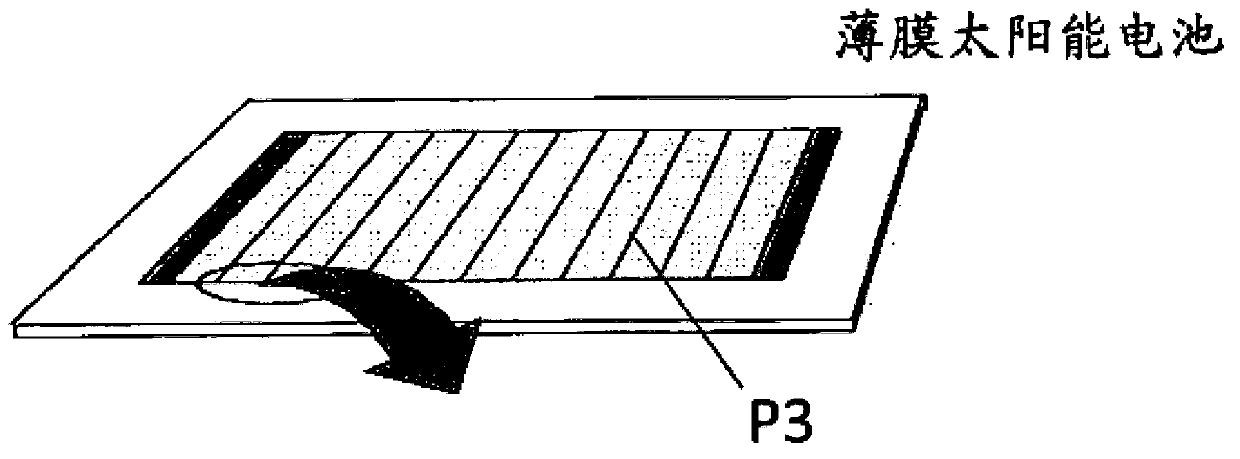
Background technique [0001] The present invention relates generally to photovoltaic solar cells, and more particularly to thin film solar cells. Background technique [0002] Thin-film photovoltaic (PV) solar cells are a class of energy devices that generate renewable energy in the form of converting light into useful electrical energy that can be used in a variety of applications. Thin film solar cells are multilayer semiconductor structures formed by depositing different thin layers and films of semiconductors and other materials on a substrate. These solar cells can be made from lightweight flexible sheets in the form of individual electrically connected cells. Figure 1A shows such a conventional solar cell sheet formed from a plurality of individual thin film solar cells electrically interconnected. The lightweight and flexible properties endow thin-film solar panels with potential applications as power sources for portable electronics, aerospace defense, and where thi...

Claims


Application Information

Patent Timeline
Patent Type & Authority Applications(China)
IPC IPC(8): H01L31/0352H01L31/18
CPCH01L31/18H01L31/0749H01L31/0322H01L31/0352Y02E10/50H01L31/0224H01L31/0392Y02B10/12H01L27/1425Y02E10/541H01L31/0463Y02P70/50
Inventor 李文钦余良胜严文材邱永升
Owner TAIWAN SEMICON MFG CO LTD
Why Eureka
Try Eureka