Semiconductor test method

A test method and semiconductor technology, applied in the direction of single semiconductor device testing, electrical measurement, and measurement devices, can solve problems such as poor contact between the test module and the needle tip, and achieve the effect of reducing the retest rate, improving work efficiency, and increasing production capacity.

Active Publication Date: 2013-05-08
CSMC TECH FAB2 CO LTD
View PDF5 Cites 7 Cited by
  • Summary
  • Abstract
  • Description
  • Claims
  • Application Information

AI Technical Summary

Problems solved by technology

[0007] The purpose of the present invention is to propose a semiconductor test method, which can solve the problem of poor contact between the test module and the needle tip, make the test value more accurate, and reduce the test abnormality very well

Method used


Image

  • Semiconductor test method
  • Semiconductor test method
  • Semiconductor test method

Examples


Embodiment Construction

[0024] The present invention will be further described in detail below in conjunction with the accompanying drawings and embodiments. It should be understood that the specific embodiments described here are only used to explain the present invention, but not to limit the present invention. In addition, it should be noted that, for the convenience of description, only some structures related to the present invention are shown in the drawings but not all structures.

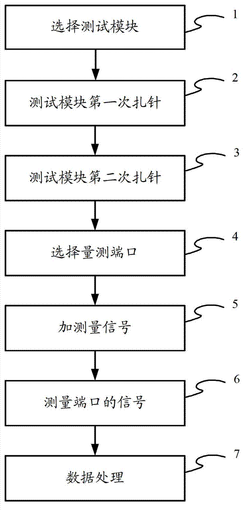
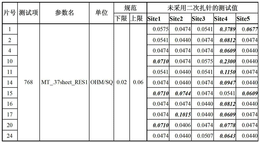
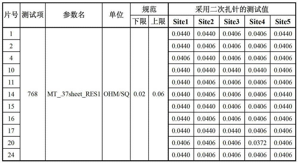
[0025] The principle of the present invention is that in the step of "needling of the test module", the second needling (Double touch) is performed on the basis of the first needling. Acupuncture pressure is expressed by the depth of the needle point when the disk and the needle point just touch. Needle insertion position and needle pressure remain unchanged. There are many ways to control needle injection. One is to use the probe table itself to control needle injection. During needle injection, the upward moveme...


PUM


Abstract

The invention discloses a semiconductor test method which comprises the following steps: a test head is provided with a probe, when a semiconductor product needs to be tested, a test contact welding pad on the product is located below the test head, and the test head is pressed downward to enable the probe to contact with the test contact welding pad in order to conduct testing. The semiconductor test method is characterized in that on the basis of a first time jab, a second time jab is also performed, and therefore the longitudinal contacting area between the probe and the test contact welding pad is increased. According to the semiconductor test method, the test problems caused by the fact that contact resistance is too large in the process of electrical parameter test are solved, test values are more accurate, retest rates of factory machines are reduced, production capacity of the factory machines is improved, and working efficiency of production lines is improved.

Description

technical field [0001] The invention relates to the technical field of semiconductor testing, in particular to a semiconductor testing method using secondary needle sticking. Background technique [0002] During the production or use of semiconductor products, it may be necessary to test the electrical characteristics of the semiconductor products first. The current test method usually adopts the push-down type, that is, the test head has downwardly protruding probes. When it is necessary to test semiconductor products, the test contact pad (PAD) on the product is located under the test head, and the test head is pressed down to make it The probe touches the test contact pad for testing. [0003] Generally, the electrical parameter testing process mainly consists of 6 steps. The first step is to select the test module; the second step is to pierce the test module, which is usually performed on the test bench; the third step is to select the measurement port, such as selecti...

Claims


Application Information

Patent Timeline
Patent Type & Authority Applications(China)
IPC IPC(8): G01R31/26G01R1/067
Inventor 连晓谦凌耀君王明陈寒顺许文慧
Owner CSMC TECH FAB2 CO LTD
Why Eureka
Try Eureka