
Multichip typesetting substrate and manufacturing method thereof

A manufacturing method and substrate technology, which are applied in the structural connection of printed circuits, printed circuit components, and electrical components to assemble printed circuits, etc., can solve the problem that the thickness of the step part is difficult to ensure, the accuracy is difficult to control, and the qualified printed circuit board sheet 502' Can't wait for the problem

Active Publication Date: 2013-04-03
IBIDEN ELECTRONICS BEIJING
View PDF7 Cites 7 Cited by
  • Summary
  • Abstract
  • Description
  • Claims
  • Application Information

AI Technical Summary

Problems solved by technology

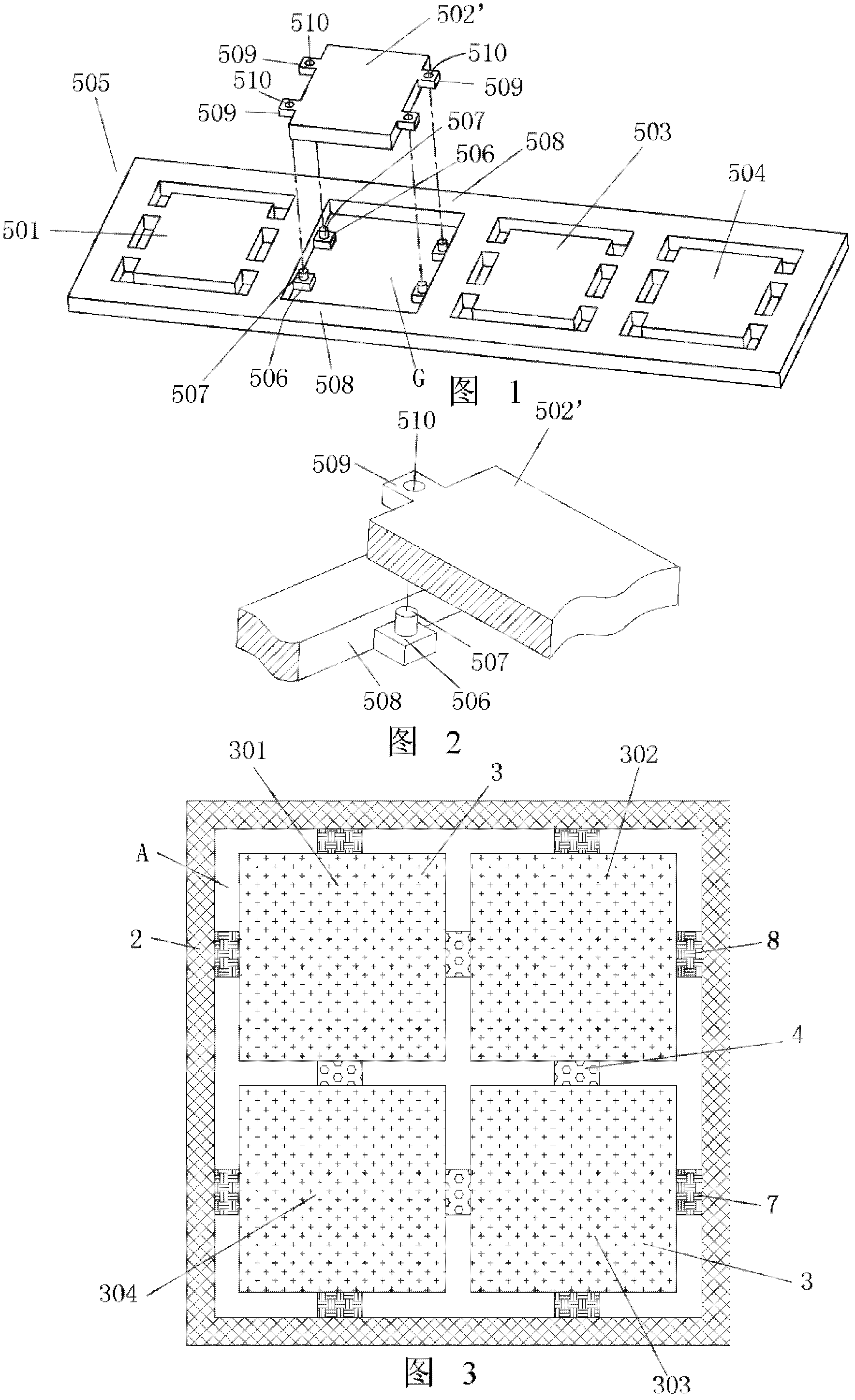
[0006] (2) Since the mutually combined peripheral buckle feet 509 and side plate connecting feet 506 are all stepped structures, and the precision of this stepped structure is difficult to control during the manufacturing process, if the thickness of the stepped parts of the two is thicker, it is easy to After the two are buckled together, the qualified printed circuit board piece 502' is higher than the finished printed circuit board 505, or the four sets of peripheral buckle feet 509 and side board connecting feet 506 used to connect the two have different thicknesses of the stepped parts. If they are not the same, the qualified printed circuit board sheet 502' cannot be installed parallel to the finished printed circuit board 505. In summary, since the thickness of the step part is not easy to guarantee, the uncertainty of the entire installation accuracy is increased, and it is easy to be installed on the printed circuit board. There are uneven steps on the finished board 505
[0007] (3) Due to the complex structure of the peripheral buckle foot 509, the buttonhole joint 510, the side plate connecting foot 506, and the tenon joint 507, when the peripheral buckle foot 509 and the side plate connecting foot 506 are small in size or the printed circuit board When the finished product 505 is a thin plate, the operable space is smaller, and there are certain difficulties in manufacturing
It can be seen from this that the single-piece part is only connected to the frame part through an adhesive. In such a structure, the connection strength, especially in the direction perpendicular to the single-piece part, is relatively low; in addition, the first opening part and the second opening part structure, when the size of the single-piece plate is small or when it is a thin plate, it is difficult to process because of the small operable space

Method used


Image

  • Multichip typesetting substrate and manufacturing method thereof
  • Multichip typesetting substrate and manufacturing method thereof
  • Multichip typesetting substrate and manufacturing method thereof

Examples


Embodiment 1

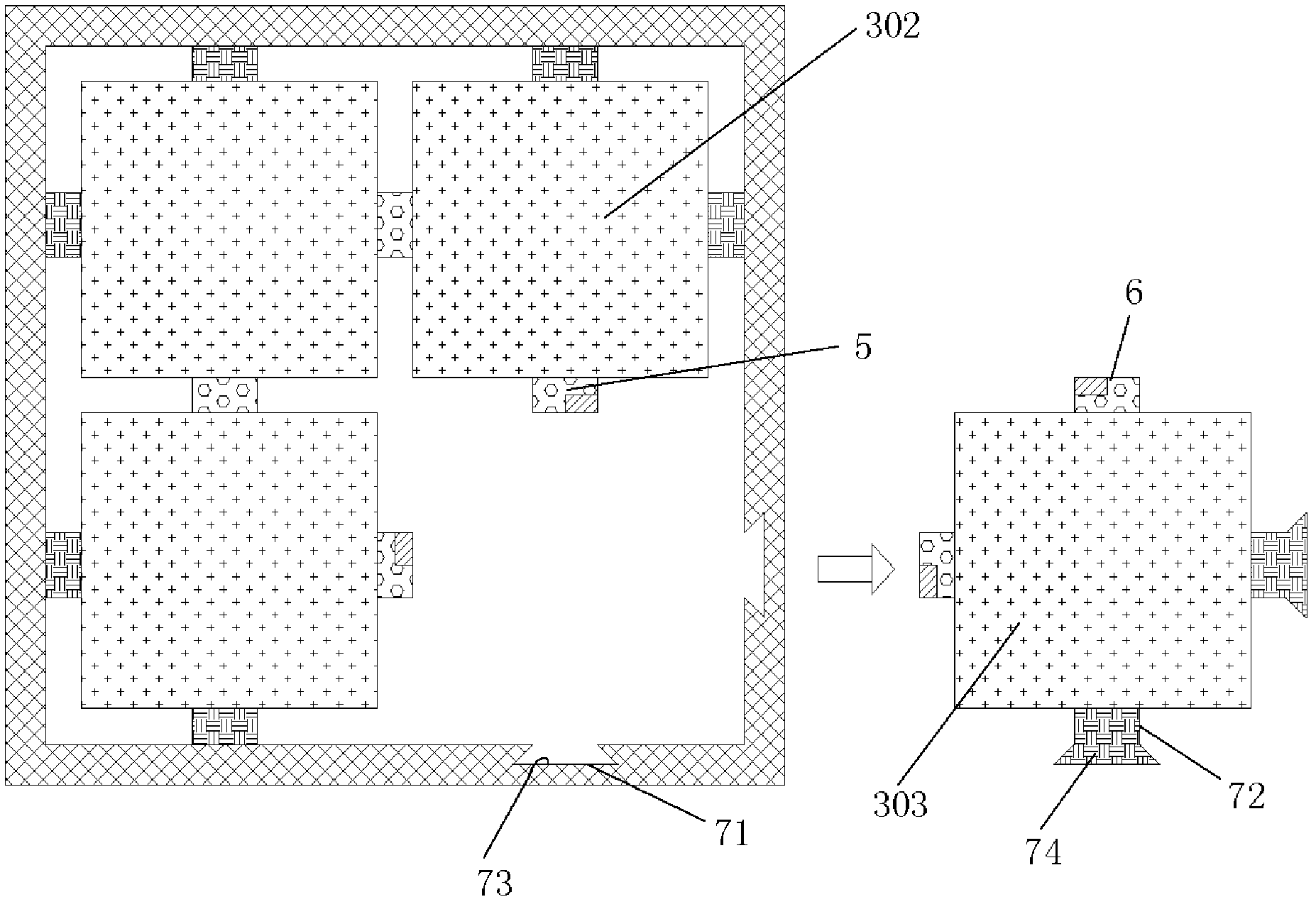
[0105] Such as image 3 As shown, it is a structural schematic diagram of a multi-piece typesetting substrate of the present invention, which includes a frame 2 and a plurality of sub-substrates 3, wherein, between the frame 2 and the sub-substrates 3, and between the sub-substrates 3 and the sub-substrates 3 are connected by a plurality of connection mechanisms 8 , the plurality of connection mechanisms 8 include at least one mechanical position-limiting connection mechanism 4 for limiting the displacement of the sub-substrate in two directions in the direction perpendicular to the frame surface or the surface of other sub-substrates, where the plurality of connections The mechanism 8 may also comprise at least one movement limiting mechanism 7 . An accommodating space A for accommodating the sub-substrate 3 is provided in the central part of the frame 2, here four substantially square sub-substrates 301, 302, 303, 304 are arranged, and each square sub-substrate is provided w...

Embodiment 2

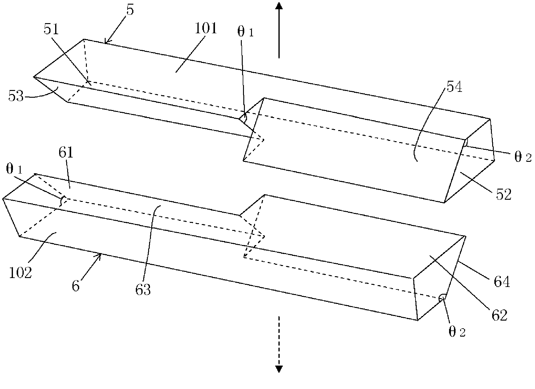
[0118] This embodiment is similar to Embodiment 1, and the same reference numerals are attached to the same structures as those of the multi-piece typesetting substrate in Embodiment 1, so the description of this part is omitted. The difference between this embodiment and embodiment 1 is: as Figure 8 As shown, after the first connecting mechanism 5 and the second connecting mechanism 6 cooperate with each other, a first notch 55 is also provided between the third connecting part 51 and the fourth connecting part 52, and the fifth connecting part 61 and the sixth connecting part A second notch 65 is provided between 62 at a position corresponding to the first notch 55 . The installation and operation of the first connecting mechanism 5 and the second connecting mechanism 6 are facilitated.

[0119] The formation of the first notch 55 here is naturally formed during the cutting process when the inclined surface 54 and the inclined surface 63 are processed. Likewise, the forma...

Embodiment 3

[0121] This embodiment is similar to Embodiment 1, and the same reference numerals are attached to the same structures as those of the multi-piece typesetting substrate in Embodiment 1, so the description of this part is omitted. The difference between this embodiment and embodiment 1 is: as Figure 9 As shown, the fifth connecting portion 61 and the sixth connecting portion 62 are multiple and interlaced with each other, and the third connecting portion 51 and the fourth connecting portion 52 that cooperate with them are correspondingly multiple, and mutually Staggered settings (figure omitted). Such as Figure 9A As shown, two fifth connecting parts 61 are arranged on the second connecting mechanism 6, and a sixth connecting part 62 is arranged in the middle. Correspondingly, two fifth connecting parts 61 are arranged on the first connecting mechanism 5. Three connecting parts 51 are provided with a fourth connecting part 52 (not shown) among them.


PUM


Abstract

The invention belongs to the technical field of printed circuit boards, and concretely relates to a multichip typesetting substrate. The multichip typesetting substrate comprises a frame (2) and multiple child substrates (3), the frame (2) and each child substrate (3) as well as the child substrates (3) are connected through multiple connecting mechanisms (8), and each connecting mechanism (8) comprises at least a mechanical limiting connection mechanism (4) which is used for limiting the child substrate (3) to move in two directions perpendicular to the surface of the frame (2). The invention also discloses a manufacturing method of the multichip typesetting substrate. The multichip typesetting substrate disclosed by the invention can reliably limit the child substrates to move in two directions perpendicular to the frame (2), therefore, the connecting strength between the child substrates, or between each child substrate and the frame, is greatly improved.

Description

technical field [0001] The invention belongs to the technical field of printed circuit boards, in particular to a multi-piece typesetting substrate and a manufacturing method thereof. Background technique [0002] General printed circuit board construction such as figure 1 As shown, there are multiple sub-boards on the motherboard of a printed circuit board. After the circuit board is manufactured, each of the multiple sub-boards of the motherboard needs to be tested. When an unqualified sub-board is found , in order not to affect the yield of subsequent component packaging, the entire mother board including the remaining qualified sub-boards is usually discarded, which will not only lead to an increase in manufacturing costs, but also cause pollution to the environment. [0003] In view of the above problems, a technique of cutting out unqualified sub-boards in the motherboard and installing qualified sub-boards as a substitute has emerged. For example, Chinese patent CN1...

Claims


Application Information

Patent Timeline
Patent Type & Authority Applications(China)
IPC IPC(8): H05K1/14H05K3/36
Inventor 韩春光乔欢杨建利
Owner IBIDEN ELECTRONICS BEIJING
Learn More