
Word line biasing circuit and storage

A word line bias and bias voltage technology, which is applied in the field of memory, can solve problems such as memory cell erasing operation logic confusion, and achieve the effects of reducing GIDL current, avoiding power loss, and weakening the electric field

Active Publication Date: 2013-04-03
SHANGHAI HUAHONG GRACE SEMICON MFG CORP
View PDF8 Cites 0 Cited by
  • Summary
  • Abstract
  • Description
  • Claims
  • Application Information

AI Technical Summary

Problems solved by technology

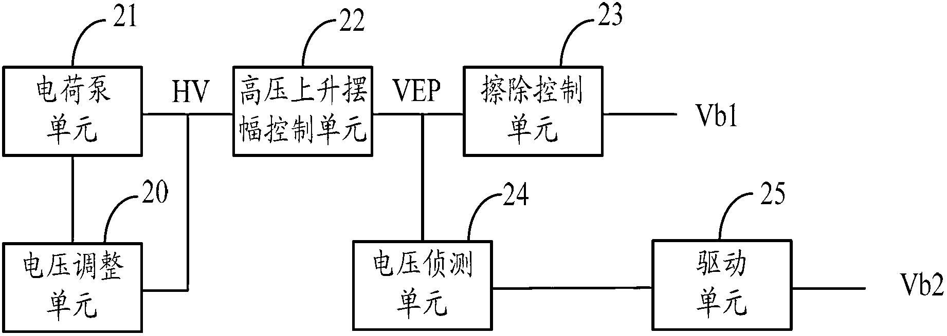
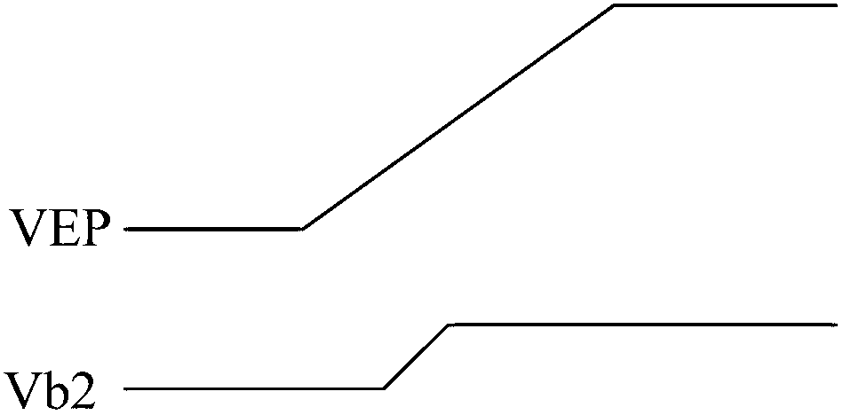
The second bias voltage Vb2 in the prior art is usually provided by a power supply voltage, image 3 Shown is a timing diagram of the stable high voltage VEP and the second bias voltage Vb2. If the voltage detection unit 24 is missing, the stable high voltage VEP and the second bias voltage Vb2 will rise simultaneously, and the first bias voltage Vb1 may be lower than the first bias voltage Vb1. The second bias voltage Vb2 causes the logic confusion of the memory cell erasing operation

Method used


Image

  • Word line biasing circuit and storage
  • Word line biasing circuit and storage
  • Word line biasing circuit and storage

Examples


Embodiment Construction

[0027] As described in the background, when performing an erasing operation on a memory cell, the word line driving unit is required to apply a high voltage to the word line, so more GIDL current will be generated in the word line driving unit. Therefore, the inventors of the technical solution consider whether it is possible to reduce the GIDL current by weakening the electric field that generates the GIDL current without excessive power loss of the storage array.

[0028] In order to make the above objects, features and advantages of the present invention more obvious and comprehensible, specific implementations of the present invention will be described in detail below in conjunction with the accompanying drawings and embodiments.

[0029] In the following description, many specific details are set forth in order to fully understand the present invention, but the present invention can also be implemented in other ways than those described here, so the present invention...


PUM


Abstract

A word line biasing circuit includes a voltage detection unit for outputting control signals, a drive unit for outputting low voltage drive signals, a first state control unit, a first level shifting unit for outputting high voltage drive signals, a second state control unit, a comparison unit, and a second level shifting unit, wherein the first state control unit is driven by the low voltage drive signal to output power voltage to a second biasing voltage output end in case that a first enable signal is effective; the second state control unit is driven by the high voltage drive signal to output target voltage to a second biasing voltage output end in case that a second enable signal is effective; the comparison unit is suitable for comparing the voltage of the second biasing voltage output end and the reference voltage and outputting comparison results; and the second level shifting unit is suitable for outputting the first enable signal and the second enable signal as per the comparison results. The word line biasing circuit provided by the technical scheme of the invention can reduce GIDL current when erasure operation is performed to a storage unit, and cannot cause extra power consumption.

Description

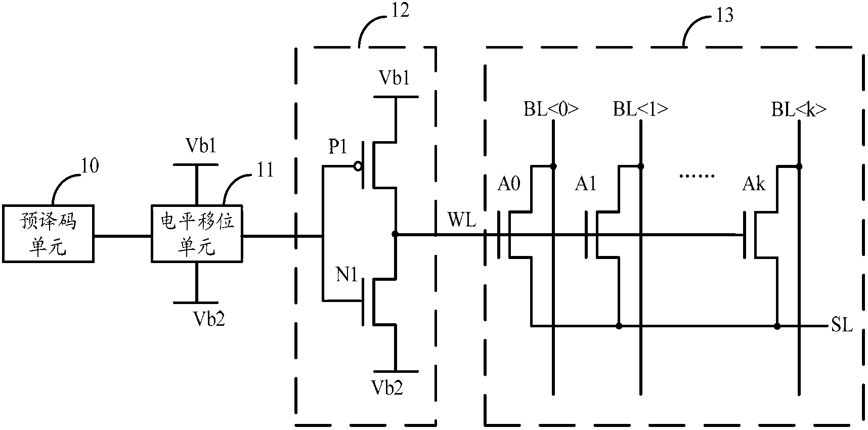
technical field [0001] The invention relates to the technical field of memory, in particular to a word line bias circuit and memory. Background technique [0002] The storage unit of the memory (for example, flash memory Flash Memory) usually includes four leads: bit line (BL, Bit-Line), word line (WL, Word-Line), source line (SL, Source-Line) and baseline (SBL, Sub-Line), which are respectively coupled to the drain, gate, source and base of the MOS transistor. Generally, when performing an erase operation on a memory cell of a memory, a high voltage needs to be applied to a word line. [0003] figure 1 A schematic diagram of a circuit structure of a memory cell array and a word line decoding circuit in a memory in the prior art is shown. refer to figure 1 As shown, the memory cell array 13 in the memory is composed of NMOS transistors, the gates of the memory cells A0, A1, ..., Ak shown are all connected to the word line WL, and the drains are respectively connected to ...

Claims


Application Information

Patent Timeline
IPC IPC(8): G11C7/12
Inventor 杨光军
Owner SHANGHAI HUAHONG GRACE SEMICON MFG CORP
Learn More