Diode chip structure for inhibiting secondary snow slide

A chip structure and diode technology, applied in the field of diodes, can solve problems such as burning out diode chips, and achieve the effects of reducing failure rate, prolonging service life, and avoiding secondary avalanches

Pending Publication Date: 2018-11-13
安徽钜芯半导体科技有限公司
View PDF0 Cites 0 Cited by
  • Summary
  • Abstract
  • Description
  • Claims
  • Application Information

AI Technical Summary

Problems solved by technology

However, as the diode voltage requirements become higher and higher, the diode chip will experience a secondary avalanche, that is, due to the avalanche electrons causing the electric field near the NN+ junction to become stronger, the diode chip will undergo a secondary avalanche near the NN+ junction, causing the diode to pass through a large current instantaneously. , generate a lot of heat, burn out the diode chip

Method used


Image

  • Diode chip structure for inhibiting secondary snow slide
  • Diode chip structure for inhibiting secondary snow slide
  • Diode chip structure for inhibiting secondary snow slide

Examples


Embodiment 1

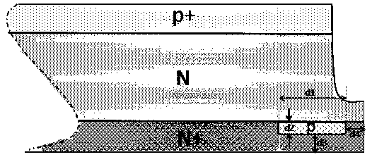
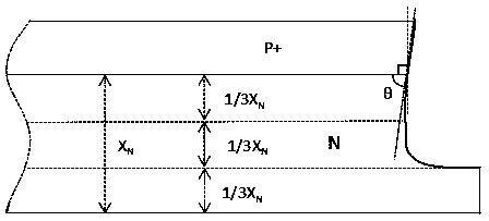
[0017] A diode chip structure for suppressing secondary avalanche, such as figure 1 , figure 2 As shown, it includes the anode P+ region, substrate N region and cathode N+ region distributed in sequence, and arc-shaped grooves are provided at the edge of the anode P+ region to two-thirds of the substrate N region, so that the edge PN junction forms an 80° ~90° positive slope angle, such as figure 2 As shown; the cathode N+ area is provided with a P-type control area.

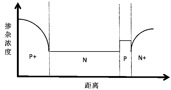
[0018] The average doping concentration of the P-type control region is 1e15-1e16cm -3 , greater than the average doping concentration of the N region of the substrate, and smaller than the average doping concentration of the anode P+ region. image 3 is the doping concentration distribution including the P-type control region.

[0019] The length d1 of the P-type control region is 1-10 μm, the thickness d2 is 0.5-50 μm, the distance d3 from the surface of the cathode N+ region is 20-90 μm, and the distanc...


PUM


Abstract

The invention provides a diode chip structure for inhibiting secondary snow slide. The diode chip structure comprises an anode P+ area, a substrate N area and a cathode N+ area which are successivelydistributed, wherein an arc groove is arranged on a position, which is two thirds to the substrate N area, of the anode P+ area on the edge, so that the junction P N on the edge form a positive skewedangle; a P-type control area is arranged in the cathode N+ area, and an average doping concentration of the P-type control area is greater than the average doping concentration of the substrate N area and smaller than the average doping concentration of the anode P+ area. Compared with the diode chip of a conventional structure, when the diode chip of the structure has the snow slide in a reverserestoration process, a great amount of electrons can migrate to the cathode N+ area, holes in the P-type control area are injected into the substrate N area to mutually compensate with the migratingelectrons, and an electric field nearby the junction NN+ can be weakened, so that the secondary snow slide nearby the junction NN+ is avoided, the failure rate of the diode in the reverse restorationprocess can be reduced, and the service life of the diode chip can be prolonged.

Description

technical field [0001] The invention relates to the technical field of diodes, in particular to a diode chip structure for suppressing secondary avalanche. Background technique [0002] Diodes, especially high-voltage diodes, although the edge of the PN junction has been properly treated, the electric field of the edge PN junction is smaller than the electric field in the body, so that the avalanche of the low-voltage diode in a short time will not cause the diode to burn out. However, as the diode voltage requirements become higher and higher, the diode chip will experience a secondary avalanche, that is, due to the avalanche electrons causing the electric field near the NN+ junction to become stronger, the diode chip will undergo a secondary avalanche near the NN+ junction, causing the diode to pass through a large current instantaneously. , generate a lot of heat, and burn out the diode chip. Contents of the invention [0003] In view of the above problems, the pre...

Claims


Application Information

Patent Timeline
Patent Type & Authority Applications(China)
IPC IPC(8): H01L29/10H01L29/861
CPCH01L29/861H01L29/10
Inventor 曹孙根王志忠张俊超芮正果
Owner 安徽钜芯半导体科技有限公司
Why Eureka
Try Eureka