Method for Forming a Sensor

a field-effect transistor and biosensor technology, applied in the field of field-effect transistor-based biosensors, can solve the problems of imposing limits on the potential sensor density and hence data throughput, carbon nanotube fets are currently not considered a mass-manufacturable technology, and suffer from a low sensitivity. , to achieve the effect of high physiological salinity level, weakening the electric field, and low sensitivity

Active Publication Date: 2021-05-27
INTERUNIVERSITAIR MICRO ELECTRONICS CENT (IMEC VZW) +1
View PDF5 Cites 0 Cited by
  • Summary
  • Abstract
  • Description
  • Claims
  • Application Information

AI Technical Summary

Benefits of technology

[0025]Biosensors comprising a FET (bioFET), and especially silicon-based such biosensors, can suffer from a low sensitivity due to electrolyte screening. Indeed, the presence of an electrolyte between the target molecule and the channel of the FET can severely weaken the electric field generated by the target molecule. This problem could be solved by detecting the target molecule in a solution of low salinity, however, for convenience, one would like to operate the bioFET at the relatively high physiological salinity level of typical biological samples. Working at the salinity level of typical biological samples also has the advantage of reducing non-specific binding to the bioFET surface.
[0026]The above objective can be accomplished by a sensor and a biosensing device having an electrolyte screening layer reducing the electrolyte thickness present between the channel of the FET and the target molecule.

Problems solved by technology

This technology imposes limits on the potential sensor density and hence data throughput due to the wave properties of light and the maximum possible pixel density of optical sensors.
Unfortunately, carbon nanotube FETs are currently not deemed a mass-manufacturable technology.
Biosensors based on more traditional semiconductors, such as silicon, would have the advantage of being mass-manufacturable, but they typically suffer from a low sensitivity.

Method used


Image

  • Method for Forming a Sensor
  • Method for Forming a Sensor
  • Method for Forming a Sensor

Examples


Embodiment Construction

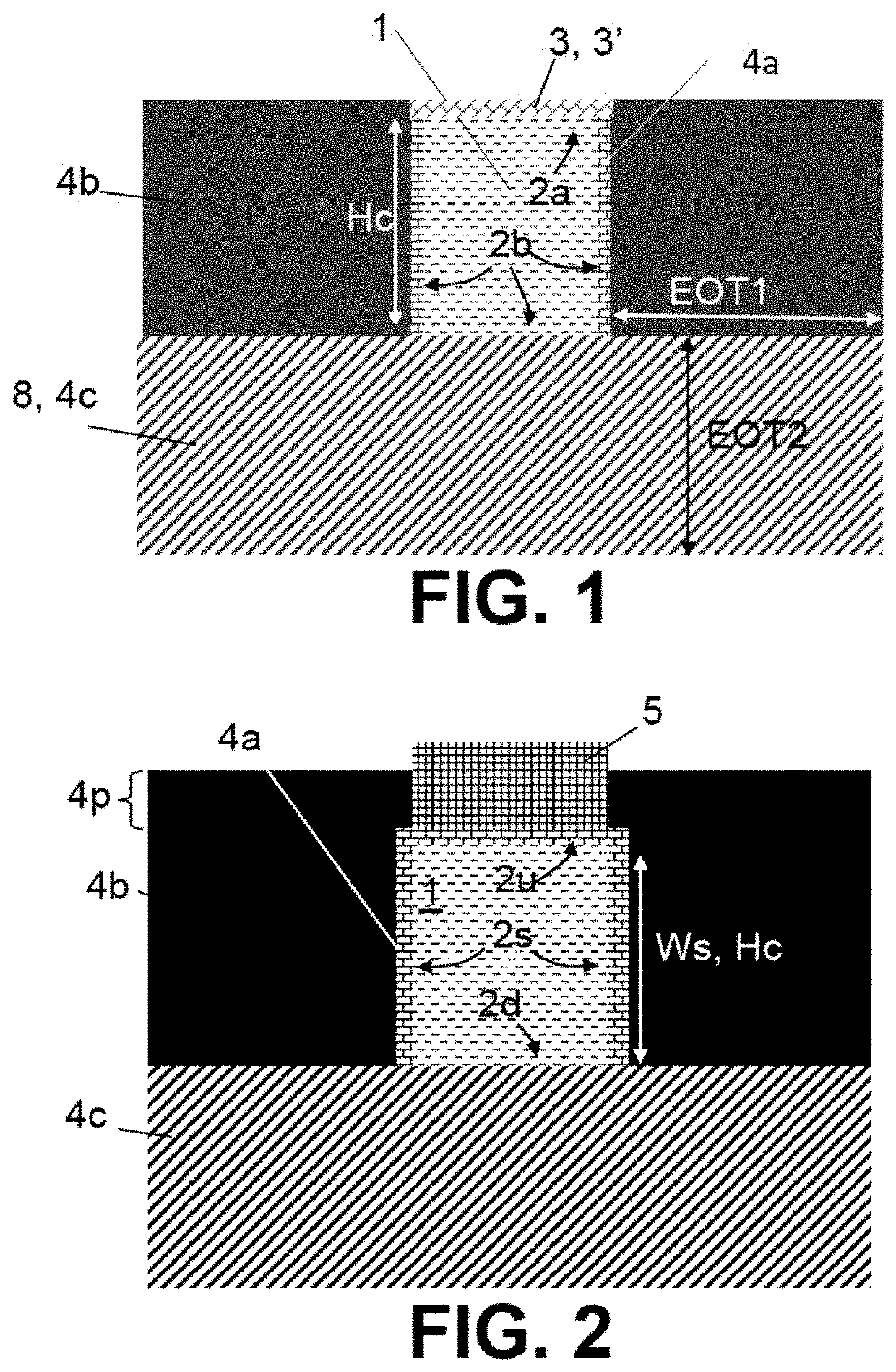
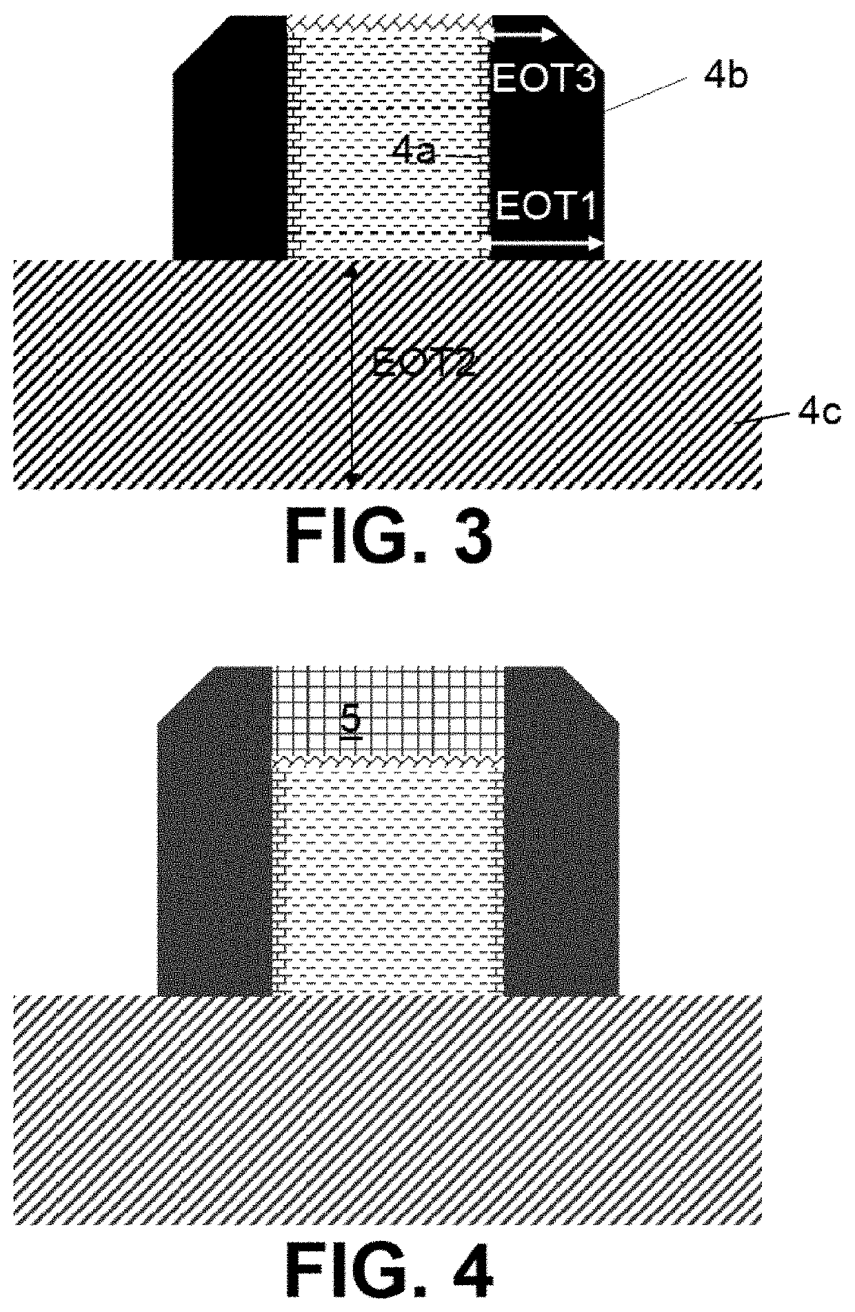
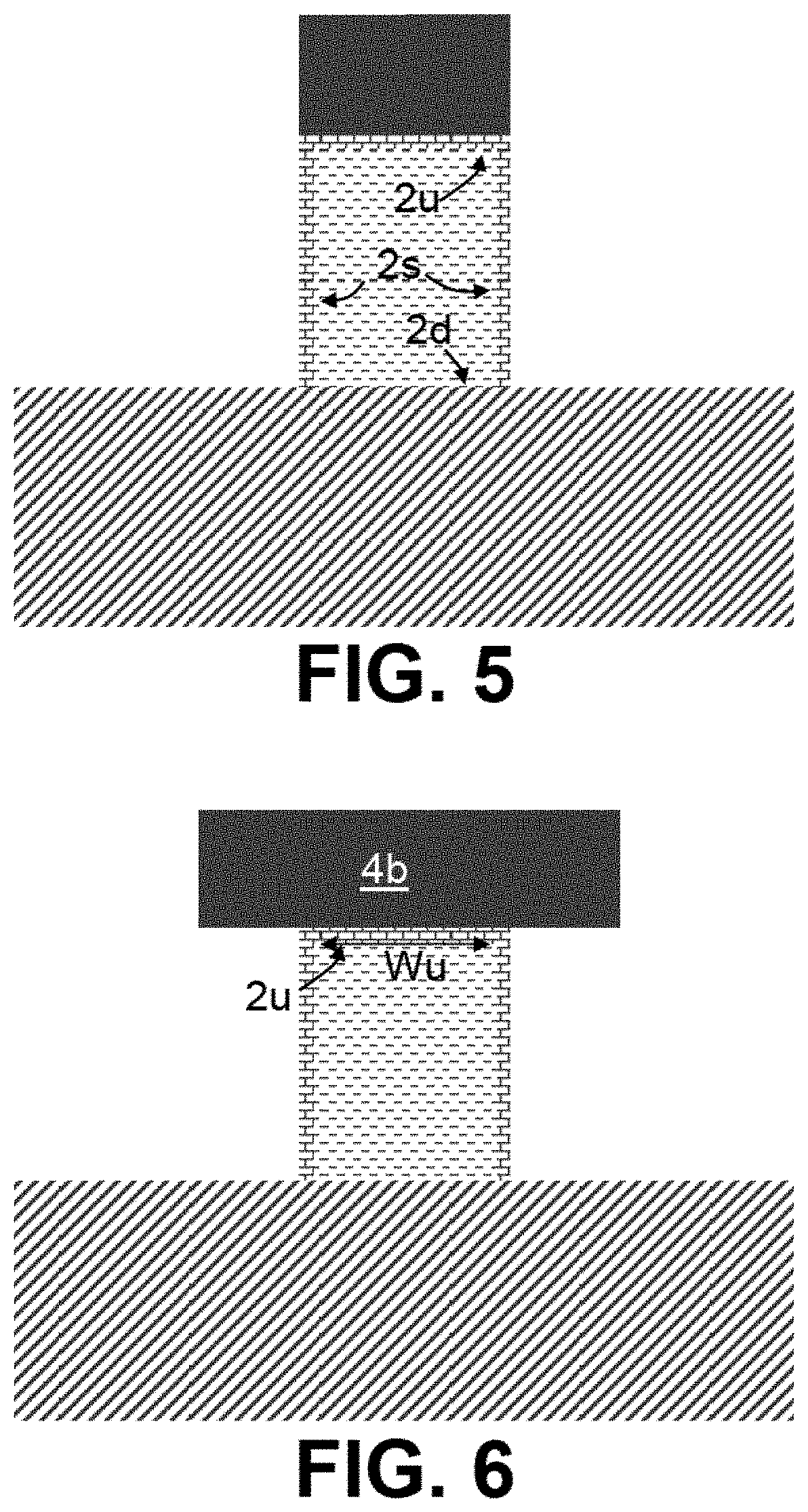
[0052]The present disclosure can be described with respect to particular embodiments and with reference to certain drawings but the disclosure is not limited thereto but only by the claims. The drawings described are only schematic and are non-limiting. In the drawings, the size of some of the elements may be exaggerated and not drawn on scale for illustrative purposes. The dimensions and the relative dimensions do not correspond to actual reductions to practice of the disclosure.

[0053]Furthermore, the terms first, second, third and the like in the description and in the claims, are used for distinguishing between similar elements and not necessarily for describing a sequence, either temporally, spatially, in ranking or in any other manner. It will be understood that the terms so used are interchangeable under appropriate circumstances and that the embodiments of the disclosure described herein are capable of operation in other sequences than described or illustrated herein.

[0054]It...


PUM

PropertyMeasurementUnit
thicknessaaaaaaaaaa
thicknessaaaaaaaaaa
heightaaaaaaaaaa

Abstract

A method for forming a sensor is provided. The method includes: providing an active region comprising a channel having: a length, and a periphery consisting of one or more surfaces having said length, said periphery comprising a first part and a second part, each part having said length, the first part representing from 10 to 75% of the area of the periphery and the second part representing from 25 to 90% of the area of the periphery; providing a first dielectric structure on the entire first part, the first dielectric structure having a maximal equivalent oxide thickness; and providing a second dielectric structure on the entire second part, the second dielectric structure having a minimal equivalent oxide thickness larger than the maximal equivalent oxide thickness of the first dielectric structure.

Description

CROSS-REFERENCE[0001]This application claims priority to European patent application no. 19210494.1, filed on Nov. 21, 2019, which is incorporated by reference in its entirety.TECHNICAL FIELD OF THE DISCLOSURE[0002]The present disclosure relates to the field of Field-Effect Transistor-based biosensors and to their fabrication.BACKGROUND OF THE DISCLOSURE[0003]Biosensors based on the detection of a single molecule, e.g by an enzyme, have been described. These devices are important as they can potentially be adapted to allow massive parallel bio-sensing. Applications, where such devices are of interest, are for instance protein analysis, proteomics (massively parallel protein identification or fingerprinting), immunoassays (antibody or antigen monitoring), and DNA sequencing, amongst others.[0004]Biosensors based on the detection of a single molecule by an enzyme are currently making use of fluorescence and optical detection. This technology imposes limits on the potential sensor dens...

Claims


Application Information

Patent Timeline
Patent Type & Authority Applications(United States)
IPC IPC(8): H01L29/66G01N27/414
CPCH01L29/6656G01N27/4145H01L29/78G01N27/414
Inventor MARTENSSANTERMANS, SYBRENHELLINGS, GEERTBARGE, DAVID
Owner INTERUNIVERSITAIR MICRO ELECTRONICS CENT (IMEC VZW)
Why Eureka
Try Eureka