
Defect detection method

A technology of defect detection and variance value, which is applied in the direction of optical testing of defects/defects, etc., can solve problems such as incorrect detection, inability to accurately reflect the actual shape characteristics of the unit chip, and reduce the accuracy and efficiency of defect scanning, so as to improve the selection performance, improving accuracy and efficiency

Active Publication Date: 2015-01-21
SEMICON MFG INT (SHANGHAI) CORP
View PDF5 Cites 1 Cited by
  • Summary
  • Abstract
  • Description
  • Claims
  • Application Information

AI Technical Summary

Problems solved by technology

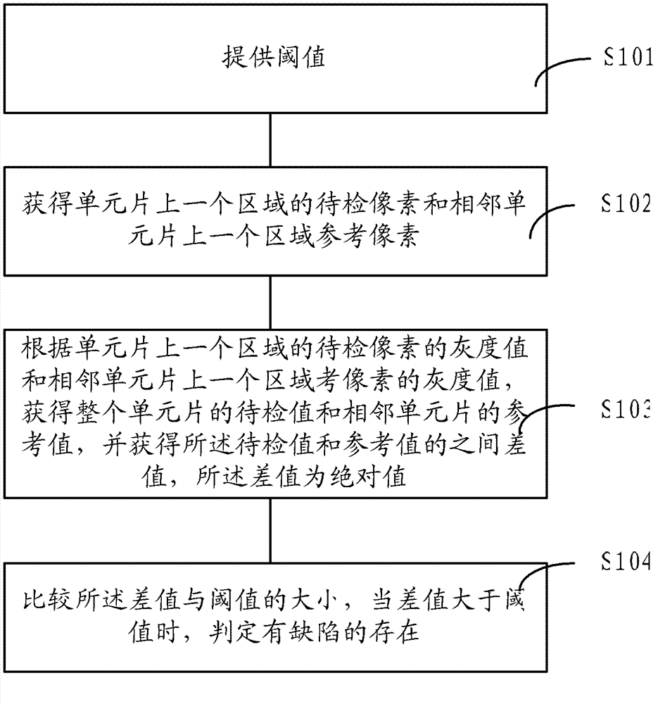
[0005] In the prior art, the value to be inspected of the unit chip is obtained according to the gray value of a region on the unit chip. Although the scanning rate can be improved, the value to be inspected cannot accurately reflect the actual morphology of the unit chip. When scanning defects, it is extremely difficult to It is easy to cause incorrect detection of defects, reducing the accuracy and efficiency of defect scanning

Method used


Image

  • Defect detection method
  • Defect detection method
  • Defect detection method

Examples


Embodiment Construction

[0034] In the process of detecting defects on the semiconductor substrate, the inventor found that in the prior art, the value to be inspected of a unit chip is obtained according to the gray value of a region on the unit chip, while the difference of the area on the product unit chip is relatively obvious. The detection value cannot accurately reflect the actual morphology of the unit chip, and it is easy to cause incorrect detection of defects during defect scanning, and the efficiency and accuracy of defect detection are low. In order to solve the above problems, the inventor proposed a defect detection method.

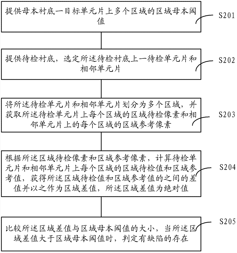
[0035] refer to figure 2 , is a schematic flowchart of an embodiment of the defect detection method of the present invention.

[0036] Step S201, providing regional mother thresholds of multiple regions on the mother substrate-target die;

[0037] Step S202, providing a substrate to be inspected, and selecting a die to be inspected and adjacent dies on the substr...


PUM


Abstract

A defect detection method comprises the following steps: providing a regional female threshold for a plurality of regions on a target unit sheet of a female substrate; providing a substrate to be detected, and selecting a to-be-detected unit sheet and a neighboring unit sheet in the to-be-detected substrate; partitioning the to-be-detected unit sheet and the adjacent unit sheet to a plurality of regions, and acquiring the regional to-be-detected pixel of each region on the to-be-detection unit sheet, and acquiring the regional reference pixel in each region on the neighboring region; calculating the regional to-be-detection value and the regional reference value of each region on the to-be-detected unit sheet and the neighboring unit sheet, and acquiring the difference between the regional to-be-detection value and the regional reference value as the regional difference, which is an absolute value; and comparing the regional difference with the regional female threshold, and determining that a defect exists if the regional difference is larger than the regional female threshold. The defect detection method provided by the invention can improve the defect detection accuracy and efficiency.

Description

technical field [0001] The invention relates to the field of semiconductors, in particular to a method for detecting defects on a substrate. Background technique [0002] With the rapid development of ULSI (Ultra Large Scale Integration), the manufacturing process of integrated circuits has become more and more complex and refined, which requires the formation of semiconductor devices with higher precision and better uniformity, and In the actual integrated circuit production process, due to the influence of different factors such as process and equipment, unpredictable defects are often formed on the surface of the substrate, such as particle defects, which eventually lead to a decrease in product yield. Therefore, in the production of integrated circuits, semiconductor Defect detection of substrates has also become critical. [0003] figure 1 It is a schematic flow chart of a defect detection method in the prior art, including steps: S101, providing a threshold value; S1...

Claims


Application Information

Patent Timeline
Patent Type & Authority Patents(China)
IPC IPC(8): G01N21/95
Inventor 叶林徐萍朱瑜杰陈思安
Owner SEMICON MFG INT (SHANGHAI) CORP
Learn More